This thread has been locked.

If you have a related question, please click the "Ask a related question" button in the top right corner. The newly created question will be automatically linked to this question.

LP8860-Q1 / Correlation of registers

Other Parts Discussed in Thread: LP8860-Q1

Hi,

My customer would like to confirm whether there is correlation of each register.

Because they have broken an IC by correlation of each register.

On the other words, can changing a register be forced another register change on the LP8860-Q1 ?

Please let me know if there is lack of the information.

Best Regards,

Kuramochi

  • Hi Kuramochi,

    Changing a register on the LP8860 will not force another register to change. Writing a register might enable/disable other registers but it won't change them.

    Only register that I can think of being linked to other registers is the CLEAR_FAULTS register which will clear the Faults registers if the fault conditions are no longer present, but those registers are read only so it's not an issue. The customer shouldn't be concern about damaging the IC due to linking of registers.

    Best Regards,

    Salome
  • Hi, Salome,I have some questions to consultation.
    LP8860-Q1 is uesd to support the backlight, which has 4 strings and every string has 11LEDs. (90mA/channel, VLED=34V,typ.)
    But ,when the Input Voltage=8.5V, the backlight starts flashing.
    the EEPROM setting is:60 0061 4F62 DF63 D164 DF65 1D66 7067 7768 7769 716A 3B
    6B 006C 0A6D 206E B06F 8470 C571 F372 E573 E374 3575 0676 DF77 FF78 3E
    when the flashing happens, read the register is:Read SPI 00 - 00
    Read SPI 01 - 00 Read SPI 02 - 00 Read SPI 03 - 4F Read SPI 04 - 00
    Read SPI 05 - 00 Read SPI 06 - 00 Read SPI 07 - 00 Read SPI 08 - 00
    Read SPI 09 - 00 Read SPI 0A - 00 Read SPI 0B - 00 Read SPI 0C - 00
    Read SPI 0D - 5F Read SPI 0E - 00 Read SPI 0F - 08 Read SPI 10 - 00
    Read SPI 11 - 00 Read SPI 12 - 10 Read SPI 13 - 04 Read SPI 14 - 6D
    Read SPI 15 - 04 Read SPI 16 - 7F Read SPI 17 - FF Read SPI 18 - FF
    Read SPI 19 - 80 Read SPI 1A - 00
    The above results show that BOOST_OCP fault happen,but I do not know how does it happen.
    Could you help to explain it ?Thank you very much.
  • Hello,

    Seems that you're reaching the Boost Imax limit, which is currently set to 4A. Could you try increasing Boost_Imax_sel register to 6A setting and see if this allows lower Vin voltage?  You can do this by writing register x70[3:1] = 100 (x04).

    I checked on one of our eval boards and it doesn't reach current limit at Vin = 8.5V under your conditions,  but around Vin =  6.5V. It could be dependent on external components that you are using (i.e inductor - recommended 22uH for 400kHz Fsw) , but I would double check that you are actually running 90mA per string. When I set 150mA/string, the current limit hits at about Vin = 8.5V.

    Hope this helps,

    Salome

  • HI Salome:
    Could you pelp to explain how it happen, reaching the Boost Imax limit?
    application condition is: 4 strings and every string has 11LEDs. (90mA/channel, VLED=34V(typ.), and the FSW=2.2MHz.
    When Vin = 8.5V, Iin=2A<4A, L=6.8uH.
    I just don't understand how it happen, reaching the Boost Imax limit?
  • Hi Salome:
    When writing register x70[3:1] = 111, and writing register x75[7:6] = 00, the backlight still flashing;
    but When writing register x70[3:1] = 010, and writing register x75[7:6] = 10, the backlight is ok.
    So I don't know whether the BOOST_OFFTIME_SEL[1:0] is useful?Best regardsSiwei
  • Hi Siwei,

    Yes BOOST_OFFTIME_SEL[1:0] needs to be set according to boost switching frequency. For higher FSW 2.2MHz, setting x75[7:6] = 10 is the recommendation.

    At 2.2MHz, the boost switching period would be ~450ns. If x75[7:6] = 00, the boost off time will be set to 131ns or ~30% of the boost period. The On time duty with these conditions probably requires higher ~80% on time. So with 131ns setting you would be limiting the on time of the boost to ~70%, and as a result triggering OCP fault.
    If x75[7:6] = 10, the boost off time will be set to 38ns or ~8% of the boost period, allowing the on duty cycle to switch as needed.

    From the EEPROM settings it seemed that the operating frequency was set to 400kHz (x71[2:0] = 011). But you're correct if FSW = 2.2MHz, this would explain why the OCP fault was triggering before actual current peak limit was reached.

    Best Regards,

    Salome
  • HI Salome,Thank you for your replay, and it is very helpful for me.
    I have other questions about VSYNC.
    When input VSYNC=60Hz, PWM=20KHz, how to set the EEPROM register?
    How to use the PLL?Thank you very much!Best regardsSiwei
  • Hi Siwei,

    I apologize for the delayed response. I'm just coming back from the holidays.

    I have attached an excel sheet SYNC calculator. It'll show all the registers that affect the clock generator control, I have already inputted the correct values for all registers to allow VSYNC 60Hz and PWM out frequency 20kHz.

    In more detail, these are the registers you would need to enable in order to synchronize PWM out with VSYNC signal:

    1.  EN_SYNC = 1 - Enable VSYNC input

    2. PWM_SYNC = 1 - Enable PWM synchronization to VSYNC signal

    3. EN_PLL = 1 - Enable PLL

    4. SEL_DIVIDER = 0 - Choose Slow PLL divider for external compensation when using VSYNC signal instead of internal osc.

    5. SYNC_TYPE = 1 - VSYNC input 50-150Hz

    From Table 2. (attached) in the datasheet, the PLL output clock and PWM output frequency are given by:

    PLL Clock Output = (VYSNC * GEN_DIV * SLOW_PLL_DIV[12:0]) / SYNC_PRE_DIV[3:0]

    Where:

    VSYNC = 60 Hz

    GEN_DIV = 1024 (for default  PWM_FREQ =0000 and PWM_RESOLUTION=00- No need to change these  registers when using external VSYNC signal)

    SLOW_PLL_DIV[12:0] = 333 or 0x14D - sets divider to get ~20kHz PWM output (60*334 = 20.04kHz)

    SYNC_PRE_DIV[3:0] = 1 or 0x00

    PLL Clock Output = (60*1024*334) / 1 = 20.52MHz

    And

    PWM Output Frequency = ( PLL Clock Output ) / GEN_DIV

    PWM Output Frequency = ( 20.52MHz ) / 1024 = 20.04kHz

    LP8860_SYNC_Calculator v1.xlsx

    Hope this helps.

  • HI Salome,An external filter should be used,yes? As showing on page 85
  • Hi Siwei,

    Yes, you are correct. Whenever using external VSYNC signal, you'll need external filter for compensation. Please refer to Table.25 for filter components selection. For discussed case above we would select the following values:

  • HI Salome,
    I set the EEPROM as suggesting, but I measured the frequence of PWM is 10KHz……
    The BOOST frequence is 2.2MHz.
  • Hi Siwei,

    Could you send whole EEPROM file? This way I can set up in the lab and check what is missing or needs to be configured differently in one of our eval boards.

    Thanks,

    Salome

  • Hi Salome,
    Sorry to reply you later, and I'm on a vacation for Chinese New Year.
    My EEPROM Setting as follow:60 0E61 6562 DF63 D064 DF65 0566 7067 7768 7769 71
    6A 3F6B 0A6C CD6D 116E B06F 8470 CF71 0772 E573 E374 7575 8676 DF77 FF78 3E
    Please help to check if any register need to be modified.Thank you very much.
    Best regards.Siwei Li
  • HI Salome,I add the application condition as folloe:VIN=12V,VOUT=36.3V;
    IOUT=90mA/string;FSW=2.2MHz;VSYNC=60Hz;
    Moreover, If VSYNC is used, can we use the Brightness Control mode "PWM input duty cycle"? or just "Brightness register" canbe uesd ?
    Thank you very much!Best regards,Siwei LI
  • Hi Siwei,

    Could you change EEPROM register x6D to 10 (currently set to 11)?

    SYNC_PRE_DIVIDER[3:0] should be set to 0x00 (which is considered as a decimal 1 in this case for calculations). This should result in the correct 20kHz PWM output.

    Also, you can use either PWM input or Brightness Register when using VSYNC signal, no limitation on which brightness control is used. 

    Regards,

    Salome

  • HI Salome,

    Thank you for your reply!

    I change the EEPROM register x6D from 0x11 to 0x 10, and the frequency is OK.

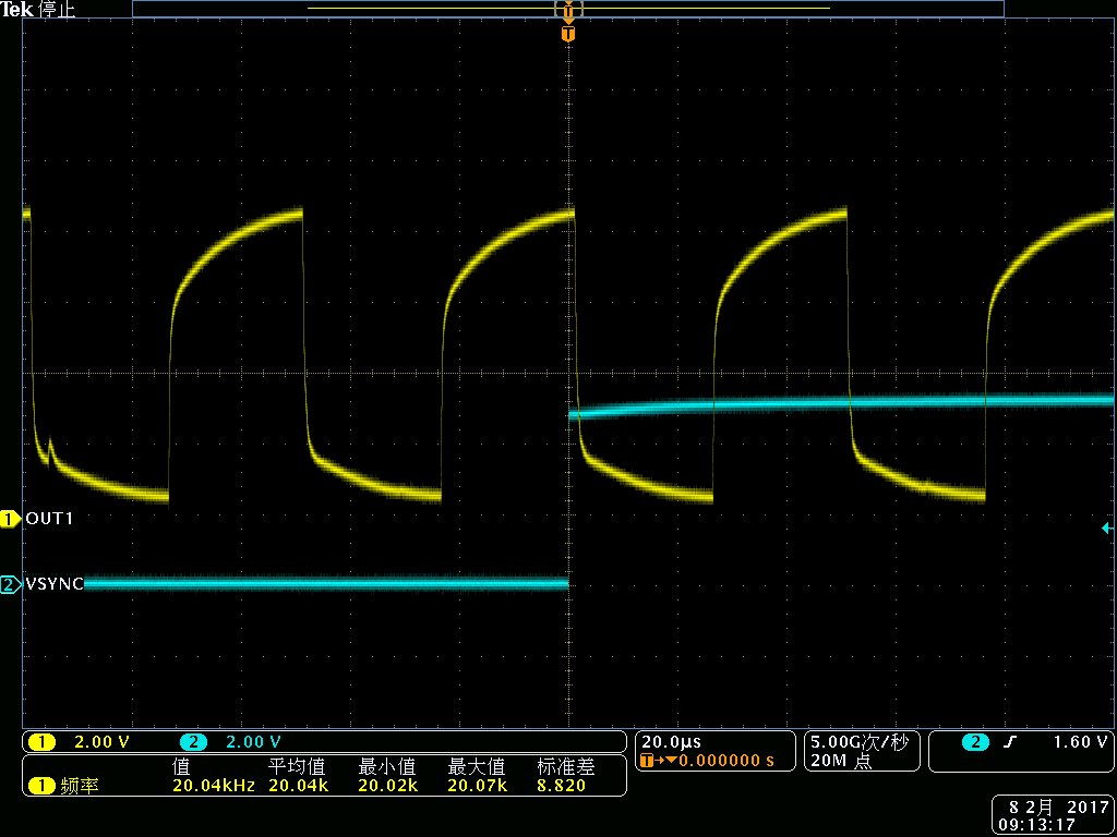
    But  PWM is not  strictly synchronization to VSYNC, as attachedment show. Sometimes can be synchronous, but sometimes can't.

  • Hi Siwei,


    A small variation in the synchronization of PWM output and VSYNC signal is expected mainly due to selected VSYNC and PWM out frequencies.


    The higher the ratio between PWM Output frequency and VSYNC signal, the higher the variation will be. So lowering the output PWM frequency can help reduce this synchronization error. Also, selecting the correct filter components as mentioned is important to improve this.


    A solution for this is to enable the PWM_COUNTER_RESET register (Address 0x6C), this will reset the PWM generator on every rising edge of VSYNC. This ensures that the PWM output will be synchronized to the start of every VSYNC cycle. But note that with this solution you still will have to account for the small error and this will add up right before the VSYNC cycle has completed so you'll most likely see shifting of last PWM pulse as shown in the screenshots below. This would mean momentary higher brightness. Although, at 20kHz this is not visible to the human eye.

    1234.tek00000.tif

    8171.tek00001.tif

    8308.tek00002.tif

    Hope this helps.

    Regards,

    Salome

  • HI Salome,

    Got it! Thank you very much!

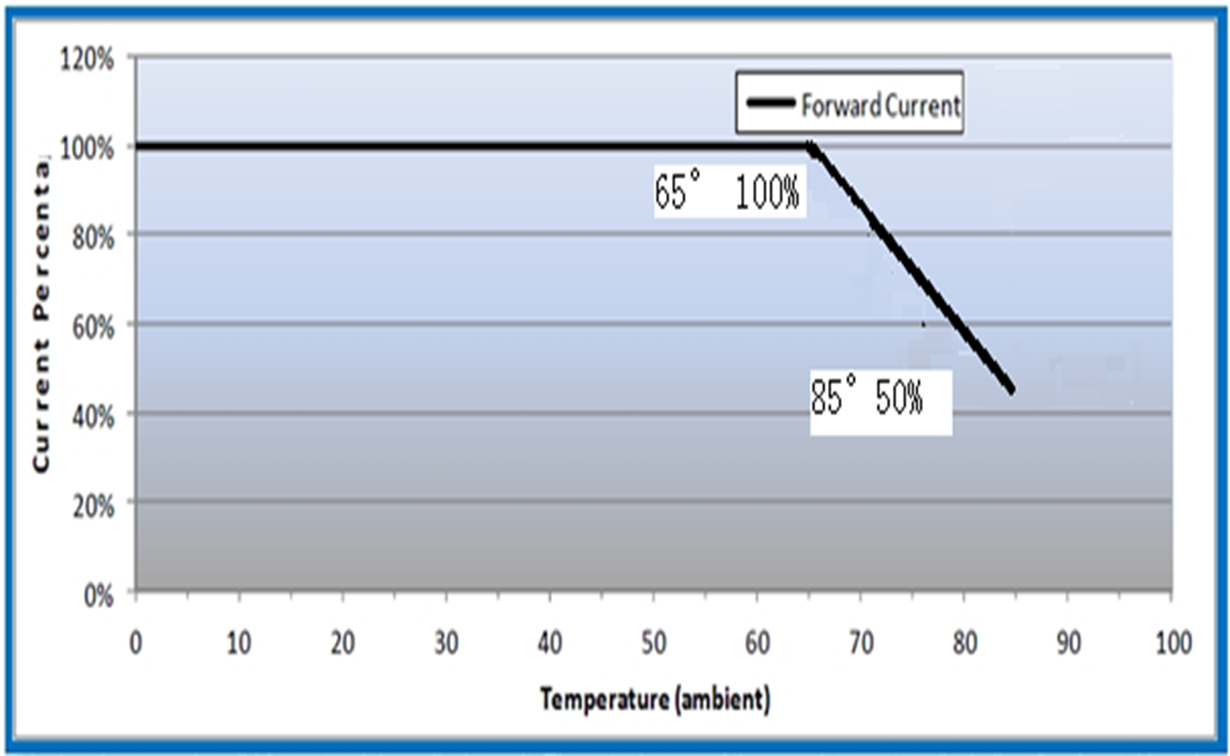
    I have another question about the External NTC Sensor. When I use the LED Current Dimming with External NTC Sensor to get the dimming curve as attachedment show, how to calculate R1 and R2 on page 37, figure 34?

  • HI Salome:
    Could you help to explain the "Dimming Ratio >13000:1 with External PWM Brightness Control" ?
    If I want Dimming Ratio =13000:1, then the input PWM frequency is ? under which mode?
    Thank you very much!Best regards,Siwei LI