This thread has been locked.

If you have a related question, please click the "Ask a related question" button in the top right corner. The newly created question will be automatically linked to this question.

TLC5916: LED Driver Problems Interacting with SN74LV125A

Part Number: TLC5916
Other Parts Discussed in Thread: SN74LV125A

Hello,

I am working on a system that consists of a large series of TLC5916IPWR's daisy-chained together on multiple boards. 

The system will involve 24 of these boards linked together, but the problem presents after just two boards are connected.

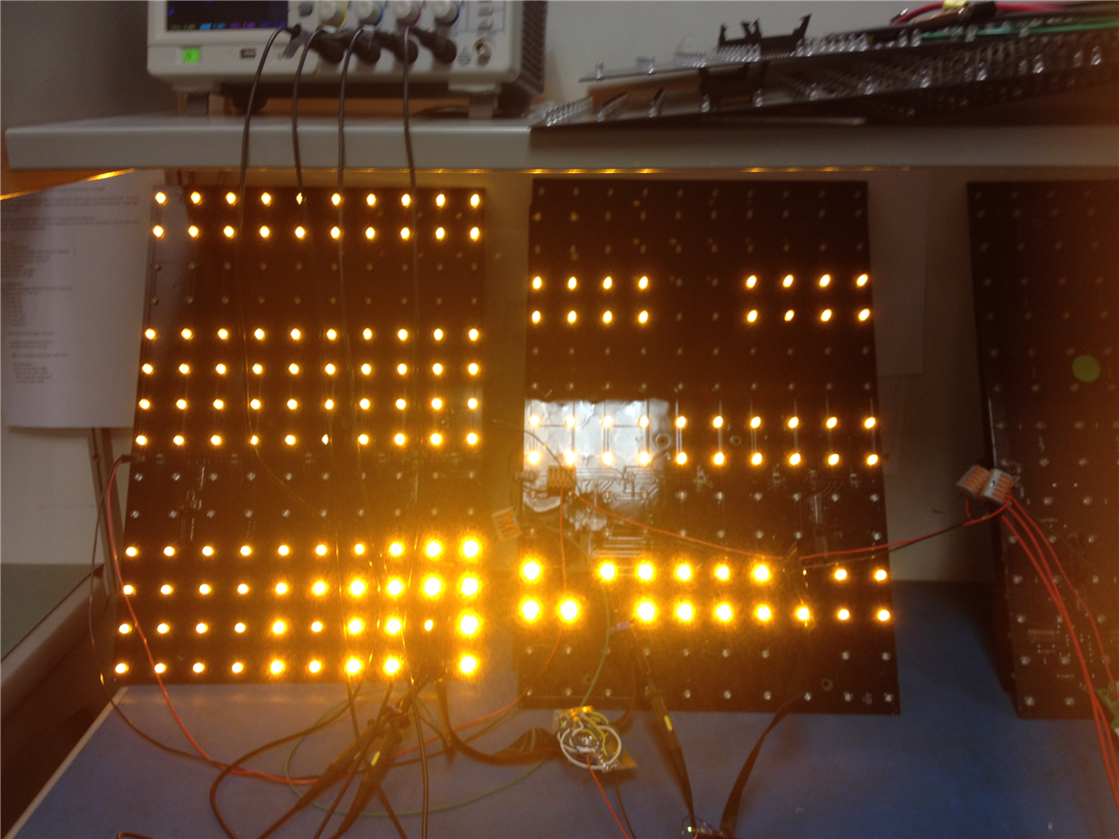
The issue I am seeing is that the digital data is corrupted between each board. The first board displays the correct pattern, but the next board lights the wrong pixels. Every board connected afterwards looks progressively worse. See two connected boards below with a simple alternating row pattern (first one on the right, second on the left. The first one has a dead pixel):

As you can see, the boards are very large (13"X19"), and are connected by a 6" ribbon cable. VSYS is provided by a 12V wall supply in testing, but it is designed to be supplied by a 12V battery. The brightness in the above image appears to vary because of narrow beam-width LEDs.

See board schematic below:

PDF version, for higher detail:

ALS_Character_ThroughHole.pdf

Missing from the schematics is that I have added 0.1uF (CHIP0402) decoupling to both buffers, an extra 10uF (CHIP1206) to the input of the linear regulator, and 47uF (Electrolytic radial lead, cut short) to the output of the linear regulator.

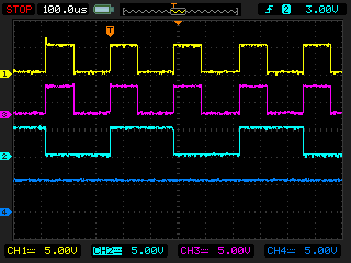
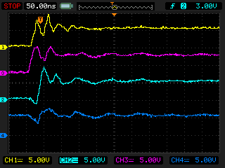
Given that the first board works fine, my assumption is the issue has to do with the interaction between the buffer and the LED drivers. Below are scope traces showing more information:

Digital Pulses:

Zoomed in on an edge:

The yellow trace is CLK out of the buffer, the purple trace is CLK into the buffer, the teal trace is one of the SDI lines out of the buffer, and the blue trace is the 5V line measured at the VCC input of U2.

Those edges aren't pretty for sure, but they appear to be within spec (and are much better since I added the 1K resistor tied from CLK In to GND).

I was hoping you would have some idea why my serial data is getting corrupted, or some tips on how to debug further. Thank you for your time.

-Spencer Allen

  • Hi Spencer,

    I need to check more details with this application.
    1. LED. How much is the forward voltage of these LEDs? How much current do you set for each channel?
    2. Device operating mode. Which mode is the device operating in? Normal mode or special mode?
    3. Topology. In the schematic, these 5 LED driver are not cascaded directly, but cascaded through the buffer. Since this device support direct cascading implementation, have you tried without the buffer?
    4. Unused channel. As this is 8 channel LED driver, I am curious why not use all channels, but left one channel for each?
    5. PCB layout. Could the PCB layout file also be sent out?

    Best regards,
    Jason Liu
  • Hello Jason,

    Thank you for the response.

    1) The LED in use is the Cree C503B-AAN. Typical forward voltage is 2.1V. the datasheet is below.

    3173.MT C503B-R-A(15-30).pdf

    With the Rext resistor at 1.4K, according to the LED driver datasheet the current set-point is 13.39mA

    2) The device is operating in normal mode only; I do not support special mode at the moment

    3) There are five strings in parallel that are cascaded from board to board. As mentioned previously, there could be up to 24 of these boards cascaded. Making it a parallel-series topology improved update rate. The clock, strobe, and enable signals need to be regenerated with a buffer every board or they degrade. The SDO pins of the LED drivers are buffered as well to prevent a race condition between the clock and data lines.

    4) This is based off of the chosen pixel configuration of the board, that being 7 rows X 5 columns. It makes sense to have one driver per column, but that does mean one output is unused.

    5) Attached below is the altium file for the layout that was manufactured from. Let me know if you need a different filetype. Note that I have altered the boards since I received them. On top of the extra capacitance I mentioned previously, I bypassed the buffer on the board and spliced two of the same buffer into the ribbon cable (after discovering said race condition). In a previous version the board was entirely single sided, if you're curious about the odd layout style.

    LED Board Layout.zip

    I should mention that In the next version of this board, I have already placed copper planes on both sides, rather than the empty space present now.

    Thank you for your time,

    -Spencer

  • Hi Spencer,

    As this TLC5916 is used in Normal mode, so all the device should be used with default setup (current gain, voltage gain), is that right?

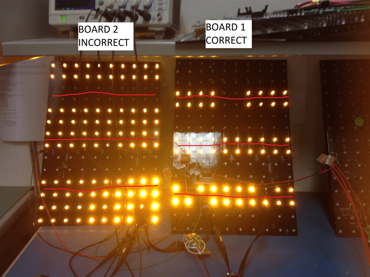
    Could you please marked the correct pattern and the wrong pattern in the first figure?
    Please also help capture the waveform of SDI, SDO, clock signal of each board (the correct board and the wrong board). BTW, please also check if the code is correctly sent into each device.

    Best regards,
    Jason
  • Hello Jason,

    you are correct, the drivers are used with default setup.

    See marked image below:

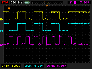
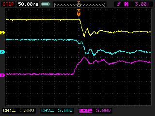
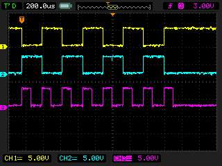
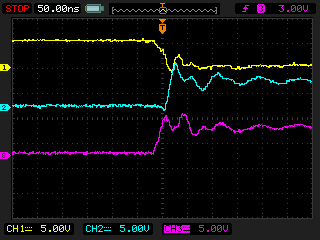
    Below are scope traces taken as requested. The measurements are taken on column 5 only, but each column should be the same. In each image, the traces are, in order from top to bottom, SDI, SDO, CLK:

    Board 1, zoomed across a single frame:

    Board 1, zoomed into the first edge:

    Board 2, zoomed across a single frame:

    Board 2, zoomed into the first edge:

    It appears the SDI of both boards is correct. But the SDO on board 2 seems to be inverted for some reason.

    Thanks,

    -Spencer

  • Hi Spencer,

    Would you mind share the code that you sent to the device? You could send me though below email if there is any concern.
    I suspect there may be something wrong with code sending.

    BTW, could you please send an image with just 1 channel of 1 device powered.

    Best regards,
    Jason Liu
  • Hello,

    The code below is written for an Arduino pro micro:

    int columnPin[] = {5, 6, 7, 8, 9};
    int enablePin = 10;
    int strobePin = 3;
    int clockPin = 4;
    int ledPin = 13;
    
    void setup() {
    
      //pin setup
      for (int i = 0; i < 5; i++) {
        pinMode(columnPin[i], OUTPUT);
      }
      pinMode(enablePin, OUTPUT);
      pinMode(strobePin, OUTPUT);
      pinMode(clockPin, OUTPUT);
      pinMode(ledPin, OUTPUT);
    
      digitalWrite(enablePin, LOW);
      //analogWrite(enablePin, 127);
      //make sure the clock starts low
      digitalWrite(clockPin, LOW);
    
    }
    
    void loop() {
      int ledState = 0;
      for (int j = 0; j < 8; j++) {
    
        if (ledState == 0) {
          ledState = 1;
          for (int i = 0; i < 5; i++) {
            digitalWrite(columnPin[i], HIGH);
          }
    
    
        } else {
          ledState = 0;
          for (int i = 0; i < 5; i++) {
            digitalWrite(columnPin[i], LOW);
          }
        }
        
        delayMicroseconds(100);
        digitalWrite(clockPin, HIGH);
        delayMicroseconds(100);
        digitalWrite(clockPin, LOW);
        
      }
      delayMicroseconds(100);
      digitalWrite(strobePin, HIGH);
      delayMicroseconds(100);
      digitalWrite(strobePin, LOW);
      
      delay(100);
    }

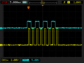
    The requested image of one pixel powered is below:

    Which was produced by the following code:

    void loop() {
      for (int j = 0; j < 8; j++) {
        if(j==4) {
          digitalWrite(columnPin[2], HIGH);
        } else {
          digitalWrite(columnPin[2], LOW);
        }
        
        delayMicroseconds(100);
        digitalWrite(clockPin, HIGH);
        delayMicroseconds(100);
        digitalWrite(clockPin, LOW);
        
      }
      delayMicroseconds(100);
      digitalWrite(strobePin, HIGH);
      delayMicroseconds(100);
      digitalWrite(strobePin, LOW);
      
      delay(100);
    }

    Regards,

    -Spencer

  • Hi Spencer,

    Refer to the datasheet figure 7, please set longer setup time for SDI data。 There might be some competition for SDI and CLK。

    I would suggest change all the delay time to much longer value, e.g. 1 second. That way you can confirm the voltages are at DC values. It might be going too fast, and the signal at the SN74LV125A (x2) aren’t as expected. This should not be a device issue.

    Best regards,
    Jason
  • Hello,

    I went through the 3-row test pattern code and replaced every delayMicroseconds(100) with a delay(1000). The resulting pattern did not change (looks the same as shown in my March 20 post).

    This makes sense, considering 100 microseconds is already several orders of magnitude above the minimum setup time shown on page 7 of the datasheet.

    Thanks,

    -Spencer

  • Hi Spencer,

    I mean SDI data should have enough setup time before CLK rising edge coming. Otherwise, there might be competition between SDI and CLK (caused wrong data).

    In the waveform you provided before, seems CLK rising edge comes at the same time of SDI data change. Please add some delay before the CLK rising edge.

    Best regards,

    Jason

  • Jason,

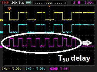
    Sorry for the delay on this response. I figured out why the waveform wasn't matching the code. I was having trouble modifying the code to add delay where suggested; nothing seemed to change it at all. But I realized I was still watching the signals *after* the buffers. So I reverted my code to back to original (with 1ms delays rather than 100us) and measured the signals on the first board, before the buffers:

    This was measured coming out of the arduino, so my code seems to be working correctly. Something else is delaying the clock signal, such that when it comes out of the buffers it is too close to the SDI line. But  with all lines buffered equally, I don't see what that could be. Any thoughts?

    Thanks,

    -Spencer

  • Hi Spencer,

    I think this should be related with the buffer, but not the LED driver. Could you try with another buffer with faster response?

    Best regards,
    Jason
  • Jason,

    I will get some parts on order, but I don't quite understand your suggestion. If every line is buffered equally, how does the response time of the buffer affect the time between the edges? I chose this buffer because it was quite fast in the first place.

    Thanks,
    -Spencer