This thread has been locked.

If you have a related question, please click the "Ask a related question" button in the top right corner. The newly created question will be automatically linked to this question.

LM3406HV-Q1: LM3406 Current issues. Delivers 0.1[A] instead 1.5[A]

Part Number: LM3406HV-Q1
Other Parts Discussed in Thread: LM3406

Hi! I'm working in a project for agricultural applications using a 50[w] led with Vf=31[V] 1.5[A]. I decided to use the LM3406 because it's high input voltage range, dimming capabilities and current.

I designed a PCB to drive the led at its maximum capability  (1.5[A]), but right now I am having issues with the output current delivered by my circuit. I am getting 0.12[A] instead the 1.5[A] that I wanted. I am using a controlled  power source that delivers 48 [V] with a maximum output current of 4[A] and a ripple of 0.1[V]. When I connect the source to the circuit a lot of noise appears, contaminating the current signal of my device. Do you have any ideas of how to solve this problem?

I notice that when I rise the input voltage (from 0[V] to 48[V]) I get a maximum current of 1[A] at 38[V], then it decrease to 0.2[A] at 48[V]. When I rise the voltage, the noise rise too, reaching a maximum value of 20[V] peak to peak. (So the input voltage varies from 38[V] to 58[V])

I also notice that when I put an input voltage over 38[V], the current through the led start operating in discontinuous mode. I think its because the over-voltage/over-current comparator system used by the driver. The input voltage noise produced also generates noise in the sense resistor voltage, exceeding the 300[mV] that this system tolerates. I Also think about "power supply interactions" between the power source and the device, but I tried with different input capacitor (according to the calculations) and the conditions did not get better. When I turn on my device, a lot of noise gets into the electrical system.

The design conditions of the project are the follows:
1) I only must use one layer (top layer in this case).

2) I need a fast response of the current. I want to test the dimmer of the drive and compare it with a high response mosfet. I want to operate the drive in a current range from 0.3[A] to 1.5[A]

3) Minimum noise injection to the electrical system.

4) Input voltage of 48[V].

I attach some oscilloscope shoots of the signals, my schematic and PCB design.

Notice that the current measures showed in the pictures are scaled (I turn more rounds in the current sensor).

I tried to solve the problem putting a parallel capacitor to the sense resistor. When I put the capacitor close to the resistor, the signal did not improve, but when I put close to the CS pin, I can get more current. (actually, that is one of the reasons why I get 1[A] at 38[V]. I also change the input capacitor to the minimum value recommended by the datasheet of the driver (equation 15). The signal improves, but the problem continues.

What do you think of my design? I am using components with a 1206 size. I designed the vias with a width of 71 [mil] for the current with 1oz of copper. I calculated that for 1.5[A] a need 7[mil] with 3oz of copper, and 12[mil] for 2oz of copper (The problem is that 3oz copper is far more expensive). The vias can produce some problems? How much far I have to put the components from the drive?
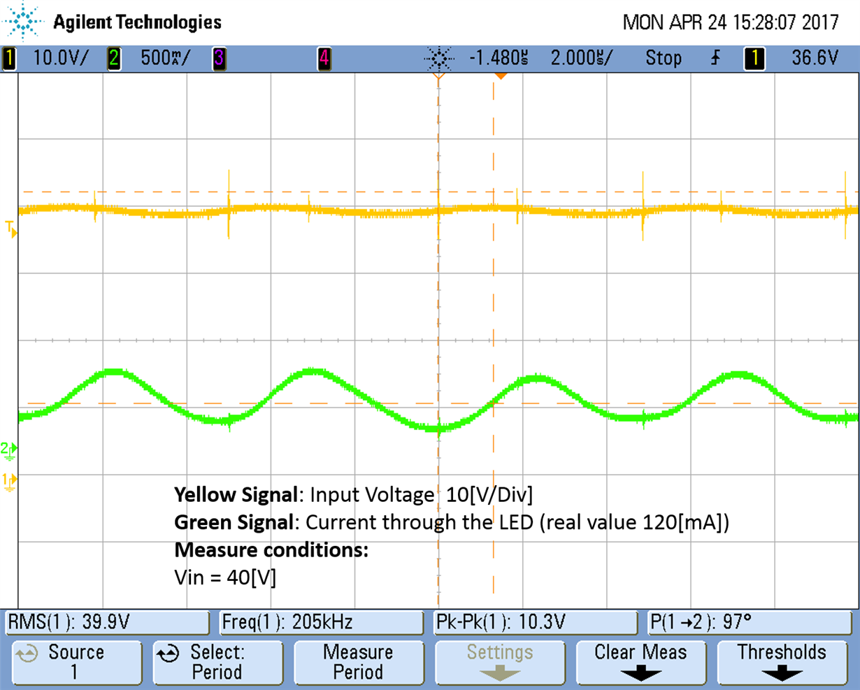
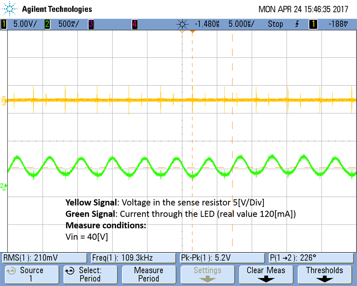
  8156.PCB2.PDF5482.2783.Schematic Prints.pdf

If you can give me some advises or recommendations I will be very grateful.

  • Hello Andres,

    I'm pretty certain I know the issue, but I wanted to ask are you really using a 100mH inductor? If so what is the saturation current rating? It needs to have a saturation current rating higher than the peak current in your design, ideally higher than the current limit of the device if you want full protection. Is that just a placeholder value? I don't see a 100mH of that case size having even close to the right current rating. If you would like me to check the full BOM for any issues I would be happy to if you can provide it. On to the two main issues I see:

    1. Input capacitance. I know there is a calculation for minimum capacitance, but that is really only for steady state operation to filter the switching frequency component and reduce the input voltage ripple to a certain level. Personally I would always at least double the calculated value if running steady state to take into account capacitor de-rating over temperature and bias voltage. If I am PWM dimming like you are I would then 10x that value again. In your case I would probably use two 10uF capacitors and make sure they are X7R, X5R, or something else with a good dielectric (not Y5V ever).

    2. Layout. Believe it or not this is one of the most common issues I see with switching regulators. Switchers generate a lot of noise so you have to be very careful with your layout (there are different rules for different topologies) or you will generate excessive noise and you will not be able to regulate properly. The most common thing you see is reduced current due to grounding and current sense errors caused by the noise. In more severe cases you will generate spikes high enough (or low enough below ground) that you will damage things.

    In all switchers grounding is the most important thing, but the grounds that matter can change. In a buck converter like the LM3406 the main grounds of interest are the input capacitor, rectifier diode (D3), current sense resistor (Rsns), and the IC. You want to have all of these grounds as close together as possible and tied together with a solid ground plane.

    The routing is also important. Think about the two cycles and where the current is discontinuous (conducts half the cycle and not the other). In the first cycle the switch will be on so the current will flow from Cin ground, out Cin+, through the internal FET, through the inductor and LED, and through the Rsns to ground. The second cycle the switch is off and the current path is from ground through D3, the inductor and LED, and through the Rsns to ground. I mention this because each cycle there will be a ground return current the opposite direction that will want to follow the forward current exactly to reduce the loop area (path of least impedance). So you need to provide some ground return path that can follow as closely as possible the forward path. This is a lot easier if you have a second layer ground plane that you can tie all of those components to with vias. If there isn't a closely following path you open up a loop that forms a radiator and can cause all sorts of noise issues. In your layout I can see that the entire board is basically a radiator.

    I also mention the ground return paths because you have to be careful where they go. You don't want them to pass directly below the IC for example. In the case of the second cycle in your layout it will pass directly beneath the IC and cause ground errors. You might be ok with it as it is but only if you used a bottom ground plane and tied all of the mentioned components directly to it with a few vias each, but it would still be good to get their grounding points closer together.

    I hope this helps. There are app notes on ti.com that give tips for switching regulator layout, those might be useful to you.

    Regards,

    Clint

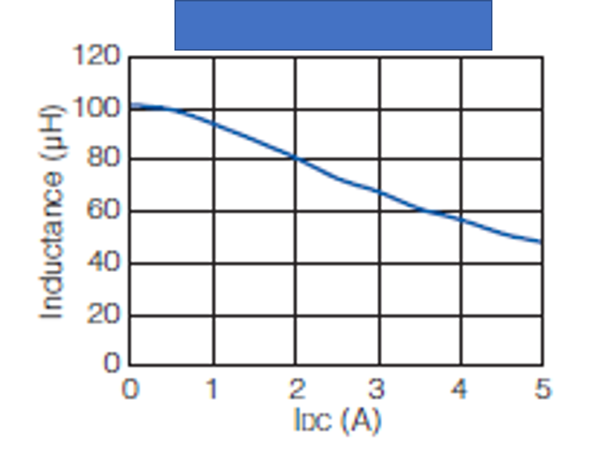
  • Thanks for your answer!  I verified the maximum current rating of the inductor that I chose, and you are right, for 1.5 [A] the inductance reduce its value to almost 90[uH].

    When I first assemble the PCB, I used a Cin capacitor of 15[uF], but the odd thing was that the noise was bigger with that value in comparison with the 0,47[uF] that I used later.

    Something I forgot to tell you, is that right now my laboratory does not have a "stove" to solder components, so I decide to put a Through-hole in the middle of the thermal pad that allows me to use a welding machine. I tested continuity with a tester, and I verified ground contact of this pad. What do you think of this?

    Do you think it is possible to create a Low-band filter connected between the source and the PCB that can solve the noise?


    I did not realize the importance of grounding! Thank you very much for your advice and fast response. I attached my bill of materials and the inductor current behavior.

    7167.BOM.pdf

    Regards,

    Andres

  • Hello Andres,

    The BOM looks fine including the inductor. I would just make sure that Rsns is a 1/3W or greater resistor, 1/4W would be pushing it. As for the DAP it should be fine as long as it is attached to ground, you could have issues if not.

    As for filtering to solve this, I honestly don't think there is any way to do it. The way you have grounds connected and routed will simply never allow you to get the full 1.5A. Layout really is critical with switchers, so much so that you really can't troubleshoot any other potential problems until you know the layout is good. Unfortunately I think the only way you will get it to work is to do a new layout.

    Regards,

    Clint

  • Hi and thanks again for all your advices!

    I read some documents of TI, you really have good stuff! I decided to re do the layout trying to follow your instructions. This time I use two layers and I chose bigger components (1210) for the sense resistance and input capacitors. I also took in considerations the paths with high slew rate currents and I put the vias in a loop that reduce the distance of the critical components. I put the components as closest as I could to the IC. I attached my new PCB design with the BOM and some layout considerations. Some of the new things that I added to my design are:

    1) I put a "Fill" under the inductor in the top layer. I read that this helps to reduce the noise of this component.

    2) I read in the datasheet that the vias for the anode of the switching diode must be thick and far from other vias. This dissuade me to put a width ground plane in the top layer of my design. I read that while more bigger the ground plane, less noise and resistance I will have in my circuit. Is that right for buck converters?

    3) I added a capacitor to the DIM pin of the IC. I think this can reduce the noise of a signal coming far from the converter.

    What do you think of this new design? The components in the bottom layer can produce interference or noise with the top layer components?

    Thanks and regards

    6281.PCB.pdf

  • Hello Andres,

    Attached are my PCB comments. It's not bad but it could be improved a little and the grounding does for sure. I'll comment on that in #2.

    1. I always use a full ground plane so there generally is ground beneath the inductor. I have always believed that is a good thing to do if possible.

    2. I haven't heard that about vias near the diode. In fact I always use them there if I have a bottom layer ground plane to connect to. The important thing is just to be careful where the current flow is and the return current paths. My suggestions will keep the loops tight and near the bottom right of the board away from everything else.

    3. That is fine.

    I think it will work well if you use my suggestions. The switching noise should then be fairly isolated and should not affect the other components.

    Regards,

    Clint

    PCBreview.pdf

  • Hello Clint,

    I did the modifications that you told me. I change the position of some components trying to get them a little far from the critical connections. I also added the vias you told me and I put a polygon ground plane in both sides of the PCB. I attached a pdf file with the new model and some things and questions that I observed while I was working in the layout.

    Thanks again!

    Regards,

    Andrés

    PCB_2.pdf

  • PCB_2review.pdfHello Andres,

    That is looking better, but I have attached a few comments in your pdf. It's mostly just about solidifying the ground planes.

    Regards,

    Clint

  • Great! I deleted all the ground paths and I connected everything through ground planes in both sides of the PCB. I attached the modifications in the file below. Do you think the design is ready?

    Thanks again!

    Regards

    Andres

    PCB_3.pdf

  • Hello Andres,

    That looks much better. The only last thing I would do would be to rotate the input caps 90 degrees counter-clockwise and try and run the trace between VIN and the input caps more directly and closer to the device. That will just shrink the loop and reduce possible generated noise.

    Regards,

    Clint

  • Hello Clint,

    I did the modifications that you recommended me. I changed some other things, like the position of the input connector in order to make the paths more direct.

    Thanks a lot for your help!

    I am aware at any other recommendation

    Regards,

    PCB_4.pdf


    Andres

  • Hello Andres,

    That looks pretty good. It should work well.

    Regards,

    Clint

  • Thanks a lot for your support and help Clint.
    You have helped me a lot.
    Regards,
    Andrés