This thread has been locked.

If you have a related question, please click the "Ask a related question" button in the top right corner. The newly created question will be automatically linked to this question.

LM3409: Which shunt dimming circuit is best for high contrast?

Part Number: LM3409
Other Parts Discussed in Thread: TPS92515,

I've been investigating using four LM3409s to use as an LED driver for an LEDEngin LZP RGBW LED.

One of the things I care about is high contrast, ideally aiming to switch the LEDs on and off fast enough that I can squeeze in 16-bit resolution per color, while maintaining a PWM frequency high enough that it's invisible. Usually I do this with a custom linear driver, but I'm intrigued by the shunt FET design for higher speed dimming.

To ground the design in some numbers, I'm planning to use a FDMD82100L dimFET with 3.3V gate voltage supplied directly from a Teensy 3.2. I plan to use a 550Hz external PWM with a minimum pulse size of 27ns to get 16-bit resolution at the optimized PWM output speed of the Teensy 3.2 controller chip. I will invert the PWM signal in software.

The LED current per channel is 700mA, the Roff is calculated to be 5.36k, the inductor is 18uH, Vin is 30V, and Rds(on) at 3.3V Vgs is about 23mohm. Coff is 480pF.

Design Notes:

I started with the datasheet design, which adds a resistor Roff2 from COFF to Vdd to keep enough current flowing into COFF to keep the system on (so I gather) at a minimum level. I calculated 1.25Mohm for that resistor. Assume diodes from all sources into the summing junction at COFF.

This seems to match R11 in the evaluation board datasheet, but R11 is noload and no mention of it is given in the evaluation board datasheet other than it being there so I am not sure if I am misinterpreting. R11 is also connected to Vin rather than Vdd.

Question: Is R11 from the evaluation board datasheet identical to Roff2 from the datasheet? Should it be connected to Vdd or Vin? Or does it not matter as long as I calculate it accordingly using Roff1*V / I_led * Rds(on)? Or should it be left unloaded for some reason?

In the evaluation board datasheet, Figure 4 shows the EN pin should be coupled to the PWM signal voltage with C9 and connected to Vdd with R4.

I get that R4 is the pullup for EN so I'm reading this as only being relevant if the PWM pulse is turned off, which will allow it to briefly shut off EN.

Question: Is coupling the PWM signal to the EN pin like this helpful? What is the point? It looks to me like it just causes EN to show the external PWM signal if it's a short pulse. Doesn't that defeat the point of the dimFET? Shouldn't EN just be tied to 3.3V to keep it active at all times when using the dimFET?

And then in the evaluation board datasheet, Figure 5 is explained as necessary if your PWM frequency is below 10kHz, which I definitely am. This is described as necessary because otherwise Coff falls too low as the voltage from Vo drops to zero and the capacitor discharges, so provides 3.3V through Roff2 when the dimFET is active to keep the off time from being too low. My calculation is that this resistor should be under 130 ohms.

Question: Did I calculate Roff2 (evaluation board datasheet, Figure 5) right? It seems weird that the value of Roff2 is independent of the PWM voltage given that it is connected to the PWM signal. It is also weird that none of the Roff paired diode forward voltages (the one from Vo, the one from PWM drive, and the one from Vdd/Vin) are relevant in calculating these values.

I think if I can understand these three questions, I can probably work out the rest.

What would you recommend doing for this application? Is this the right chip for the job?

References:

Part Datasheet - http://www.ti.com/lit/ds/symlink/lm3409.pdf

  • Sorry, the link to the Evaluation Board Datasheet got truncated or something.

    www.ti.com/.../snva390d.pdf

    Also, for my second question I noticed on re-reading that because the PWM signal is inverted, turning the shunt FET off (LED ON) should pulse the Coff voltage low rather than turning the shunt FED on (LED OFF) pulsing the Coff voltage low. I don't really understand Coff, but maybe that is a clue to my confusion about the point of the EN coupling when doing shunt dimming.
  • Hello Brian,

    Hopefully I can make this easy: Don't refer to the EVM at all for shunt FET dimming. It wasn't understood as well as it could have been when the EVM was made and EN coupling and everything else isn't really necessary. Use the datasheet for your calculations and the ROFF2 connection. VIN (if stable) or an external VDD can be used, it just changes the calculation as you mentioned. The reason for the second ROFF resistor is simply because if the output drops to less than 1.24V with the shunt FET on (which is almost always will) you want to provide a charging path so that you are not hitting maximum OFF time which can negatively affect the dimming. You want to match the inductor current peak-to-peak ripple during the shunt FET on and off times so that you have the same current level at each transition each cycle. You can refer to the TPS92515 datasheet as it has a little more information about this and they use the same control circuitry with the only difference being a slightly different ROFF threshold.

    I hope that helps.

    Regards,

    Clint

  • Thanks so much Clint, this helps a lot. The TPS92515 datasheet is a lot clearer to me, is it the most recent chip? Do you think the TPS92515 might be more appropriate?

    I'm only running at 700mA, and my primary goal is to make it compact since I have to fit four of these modules onto a pretty small control board.

    Some followup questions inspired by the TPS92515 datasheet --

    In Figure 27, they show the dimming linearity with different methods. I'm curious as to what is limiting the dimming contrast ratio for the Shunt FET version above about 10000:1. Is it limited by the high frequency (i.e. by the dimFET) or by the long off time?

    In the interim since I asked this, I also realized I can't use the dimFET I planned on due to the dual FETs not being independent, and am now looking at the BUK9K6R2-40E (http://assets.nexperia.com/documents/data-sheet/BUK9K6R2-40E.pdf) with a somewhat lower Ron, faster switching times, and lower gate threshold voltage. From looking at the delay times, I'm suspecting that my minimum pulse length needs to be at least ~100ns. To get 16-bit dimming, should I just combine lower resolution PWM dimming with current dimming? That seems unlikely to be very linear, but does that make more sense to do in practice? I'd rather just stick to PWM dimming, so I can also lower the PWM frequency but if the contrast ratio is limited by the off time being too long that seems less likely to work. If I should use iadj to get the full range I should design my board differently, so some advice on that would be great!

    Regarding Roff2

    For selecting Roff2, the equation in the LM3409 datasheet says I should use a 3.16Mohm resistor for Roff2 since my dimFET on resistance should be about 0.008 ohm, Vdd is 3.3V, and ILED is 700mA.

    For the TPS92515 version of the equation, my inductor ripple current is 187mA according to webbench, my inductor is 18uH, Ron is 0.008 ohm and my LED current is 700mA, so I get a t_off-shunt of 4.77 microseconds. With the Coff of 470pF and a 3.3V VDD, this works out to 28.1kohm for Roff2 instead.

    As best I can tell the difference should just be the 1V vs 1.24V threshold. But even using 1.24 in place of 1 in the ln(1-(1/Vdd)) only gives a Roff2 of 69.6kohm.

    These are so different that I'm afraid I'm not sure which to use.

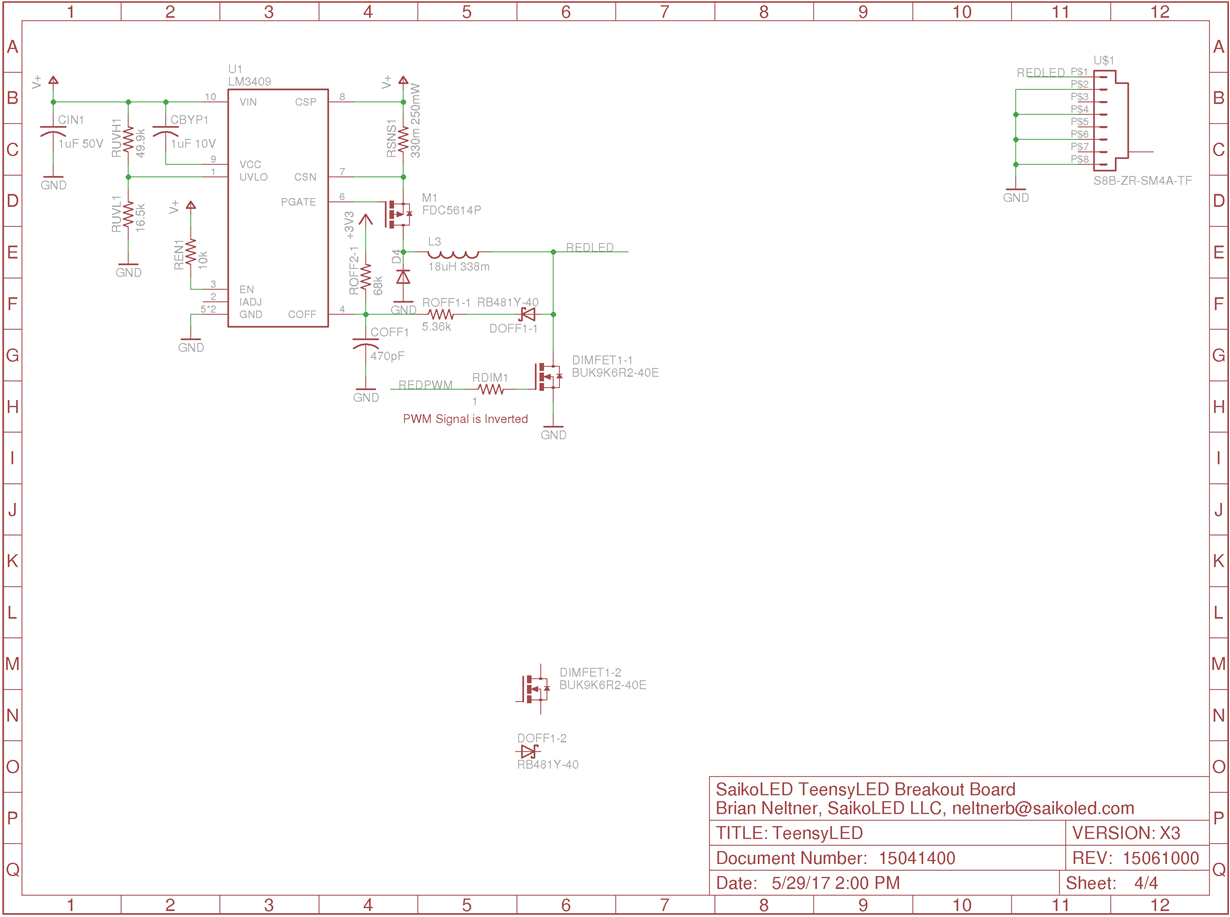
    I attached an image of my current design, to help clarify and maybe you can identify any issues...

  • Hello Brian,

    The TPS92515 is a newer device and would be a smaller solution since it is integrated. As for the equations I would trust the newer datasheet, I am not sure of the accuracy of the older datasheet. The 515 also has an excel calculator available on the web. In the end with either you generally need to monitor the inductor current and tweak Roff2 a little on the bench.

    If you are interested in the 515 check out the following link for a reference design that gives a lot of information on PWM, shunt FET, analog, and PWM/analog combo dimming. Depending on the switching frequency and input/output voltages you can be limited with analog dimming due to the minimum on time of the switch. PWM and shunt FET dimming are generally limited by the rise and fall times of the output current.

    Regards,

    Clint

  • Hi Clint,

    I am considering trying to utilize 28 lower voltage outputs rather than four.

    Do you have any recommendation for how I might do this in a simpler way than implementing 28 full LM3409 layouts?

    Is there a device which might output a constant current in the 350mA to 1A range for many channels with a small number of parts, which I could then use a shunt FET for dimming with? Since I no longer need the current source to be dimmable, perhaps that expands the options to multi-output voltage regulators with a sense resistor? Or do you think just having many drivers is a better option?

  • Hello Brian,

    350mA to 1A per LED is pretty high current for any multiple output type regulators, they are generally 350mA max or much less. Obviously 28 channels of the LM3409 (or TPS92515 if you want to save cost and space) would work really well, particularly if you need individual control of each LED. But I'm not sure of your exact requirements for control. If you have multiple LEDs that will always be at the same forward current you could stack them in series at the output of the LM3409/TPS92515 and put a separate shunt FET across each to PWM them individually. What will be required really depends on how independent each of the 28 outputs needs to be from the others.

    Regards,

    Clint

  • Thanks Clint, fair enough. The highest multi-channel device output current I found was 150mA, but if there's one at 350mA I would definitely use it.

    I would be using the same forward current for each LED, your solution sounds very good of connecting them in series and using a shunt FET to short out the inactive LEDs in the chain. That's very clever! Thank you for the idea, is that a common solution?

    With regards to Roff2 calculation, would you agree that because the purpose is to avoid reaching the maximum OFF-time, it is only relevant in a situation where all LEDs have been shunted? And thus I can use the same equation given in the TPS92515 datasheet except using n*Vshunt in place of Vshunt where n is the number of series shunted LEDs?

  • Hello Brian,

    Yes, Roff2 is only for all of them shunted and that is how you would calculate it. In fact, if n*Vshunt is greater than 1.24V (say >1.5V to give headroom) then Roff2 wouldn't even be needed. But that depends on n and the Rds(on) of the FETs. It is a common solution and has been used in a variety of applications. The LM3409 and TPS92515 are some of the only parts capable of it due to their fast response time.

    Regards,

    Clint

  • Hi Clint!

    I've had a chance to start working through the details a bit more, and am trying to find a good method to generate the PWM control signals with high enough output voltage to control the MOSFET highest in the chain of shunts, with low enough output impedance to drive the MOSFETs quickly.

    I was originally thinking to use one of your large-display drivers with many current sinking outputs and a pullup resistor to 18V, but it occurred to me that at the currents these can sink and with the resistor in there that the gate charge on the MOSFET will end up limiting the switching speed to 1us+ just due to the time it takes to place ~10nC onto the gate or remove it.

    But my control chip doesn't have enough PWM outputs to handle it by itself.

    Is there a multi-output driver chip from TI which would let me generate the PWM signals with bipolar operation? I can envision simply using a line driver to take the PWM output voltage up to 18V, but actually generating the PWM signals with low impedance in both directions is looking tricky. Even if I'm just using the current sink chips to generate 3.3V logic signals, this feels like it will be too slow at a 10mA current.

    Brian

  • Hello Brian,

    I'm not an expert on how to control multiple series FETs like this, I just know it can be done. But if I calculate correctly to drive a 10nC FET at 550Hz only requires 5.5uA per FET average.

    You could also try NPN/PNP totem poles to increase drive. Tie the gates together and put the NPN to high voltage and the PNP to ground. When you pull high the NPN turns on and the output (between the two) pulls high and when you pull the gates low the PNP turns on and pulls the output low. I hope any of this helps you.

    Regards,

    Clint