This thread has been locked.

If you have a related question, please click the "Ask a related question" button in the top right corner. The newly created question will be automatically linked to this question.

TPS92641: Questions regarding circuit dimensioning

Part Number: TPS92641

I am currently evaluating TPS92641 LED drivers on prototype boards. The application scenario is as follows:

- Input voltage: 12-28V

- Output voltage: 2-5V (single LED)

- Output current: 500mA - 5A

- Switching frequency: currently 300kHz (will maybe lowered to 250kHz to ensure minimum on time in worst case operating conditions)

- Dimming: Analog + UDIM (1.5kHz)

The driver is functional, but both switching frequency and duty cycle are not stable. When the Rf series resistance is set to 470Ohm, I see double switching pulses (it looks like the overcurrent behaviour but with shorter gap in between the pulses). By increasing the resistance to 10KOhm this behaviour can eliminated.

My sense resistor is set to 20mOhm to keep power dissipation in an acceptable range for the higher output currents, which the circuit should be able to drive. Is it necessary to increase Rf when using such low resistance values for current sensing ?

Regarding the compensation capacitor: Which value would be applicable for my design ? Is 100nF the right choice for the PWM dimming application by using UDIM ?

Another question is related to the dimensioning of the on-time circuit. Is there any lower limit for the Con capacitance value ? I want to keep the power dissipation of the Ron resistor as low as possible and therefore it is necessary to use a capacitance <1nF, which is used in all reference designs I found so far.

The entire circuit is depicted in the follow schematic, T15 and C36 are not populated. I would be grateful for comments and hints regarding the dimensioning.

  • Hello,

    To answer your question:

    1. A 20mohm sense resistor is fine. You should not need to increase Rf either. I suspect it is a layout issue and the extra filtering provided by the 10k is masking it to some degree. I would be happy to look over your prototype layout and comment if you would like. I believe there are layout guidelines at the end of the datasheet you could compare to as well if you would rather.

    2. 100nF or more is fine for any application. The only time you may want to change that is if you need fast IADJ bandwidth which is rare. In that case you can actually lower it, but I don't see the need here, especially when you already have a 10uF cap on IADJ.

    3. That resistor should not dissipate much at all even with 1nF. But yes, you can use less. Just keep in mind at some point pin capacitance and other parasitic capacitances may become a significant factor the lower you go. Ron may need to be tweaked accordingly. I would recommend maybe 100pF absolute minimum with 220pF to 470pF being more reasonable. Your choice.

    Regards,

    Clint

  • Thanks for your response,

    I will keep the values of 20mOhm for the sense reistor and 100nF for the compensation capacitor (IADJ bandwith is not a concern).

    Regarding Ron:

    At first I used 6.34KOhm - 1nF for the ramp circuit. With this resitance value, I observed a hot spot on the resistor when looking at the circuit with a thermal vision camera. At 28V its expected power dissipation during off-time is (28*28)/6340 W = 124mW and during on-time slightly lower when charging up the capacitor to the feedback voltage. In average the power dissipation is beyond 100mW, which is inacceptable for my case. The package limit for 0603 is 100mW and I always keep some headroom. Furthermore on my board, there are 4 LED drivers and the dissipation of the ramp circuits would sum up to 400mW in total.

    I am also quite sure that my major problem is noise on the current sense signal. Please find the layout below (2-layer, yellow top, blue bottom, flooded areas are GND), thanks in advance for any comments and hints.

    By the way, the LED unit is connected to the driver PCB with a cable of approx. 30cm length. Relocating or adding components to the LED PCB is rather difficult.

  • Hello,

    Your layout overall is actually pretty good. The only thing that really concerns me is the VCC capacitor and the fact that it only has one via to ground. The placement of the via is a little concerning too, but mostly because there is only one. VCC may only be supplying an average of 20mA or 30mA (depends on Fsw and Qg) but the peak currents in the VCC cap to turn the FETs on/off and charge the BOOT cap are much higher. They could be a few amps peak each cycle, maybe more.

    So this concerns me for two reasons:

    The first is that the via is right next to the CS pin. Those kinds of peak currents through a single via are going to generate a lot of noise and it could be radiating into the CS pin.

    The second is that with those peak currents and the resistance/inductance of a single via VCC could be collapsing some each cycle which could cause a lot of noise on VCC and could also cause a lot of noise on the gate drive signals. LG happens to be right next to the CS pin and the CS trace that connects to the current sense resistor.

    You should be able to probe VCC, HG, and LG to see if there is excessive noise on them. If so then it may be the placement and the single via. In that case I would take the VCC cap/boot diode combo and rotate them 90 degrees counter-clockwise and get the VCC cap ground connected to the ground plane the input caps are on.

    Regards,

    Clint

  • Thanks again for your helpful response. I modified a PCB using your suggestion (connecting the VCC cap to the switching GND) and was able to reduce the Rf resistance value. I was not able to go down to 470Ohm, but with 1KOhm no more double switching pulses occured. For the next PCB revision I am not sure which of the two approaches would be better:

    1. using your suggestion and connecting the VCC cap

    2. reinforcing the GND connection of the VCC cap by adding vias and also increasing the distance to the CS trace

    My concern is, that when using the first approache, noise from the "dirty" switching GND is electrically coupled into the voltage reference system of the IC. Still both duty cycle and frequency are varying from cycle to cycle (I would say approx. 5-10%) and I have no idea if this behaviour is normal and how to improve it.

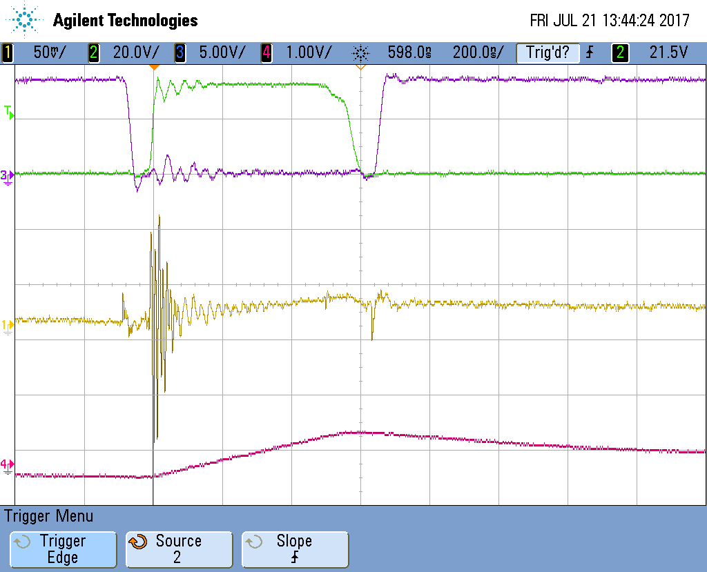
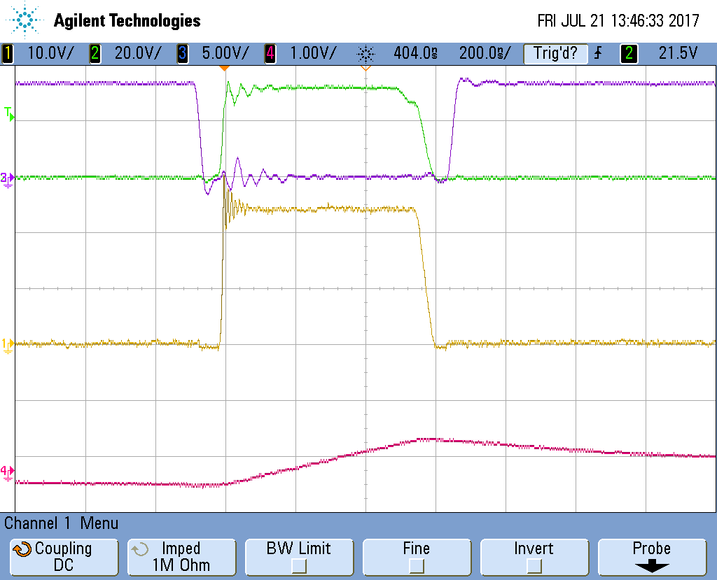
    Below are measurements taken on the modified PCB:

    green: HG, violet: LG, yellow: voltage across the sense resistor, red: inductor current

    green: HG, violet: LG, yellow: switch node, red: inductor current

    As you can see in the schematic, I already increased the HG gate resistance to 22Ohm to reduce the overshoot and ringing on the switch node to an acceptable level (approx. 30V peak), since 40V MOSFETs are used on the board. Also I tested a small snubber circuit which eliminates the ringing, but it is not populated right now.

    Do the measurements look normal ? I would be grateful for further comments.

  • Hello,

    Either way should work ok. The VCC cap ground is part of the "noisy" ground which is why it needs to be tied to the ground plane really well. Rerouting the CS trace a little further away couldn't hurt either.

    But your measurements look fine from what I can tell. A few switching cycles in a scope shot would be more telling. However, to answer your question on the 5% to 10% variation each cycle it is likely normal. The error amp is chopping (see the datasheet for more info) so it swaps polarity each cycle. This is to eliminate the input offset which is what makes the device so accurate. You can't get total CS offsets of +/-600uV worst case without doing that.

    Regards,

    Clint