This thread has been locked.

If you have a related question, please click the "Ask a related question" button in the top right corner. The newly created question will be automatically linked to this question.

LM3409: Unexpected Output Current

Part Number: LM3409

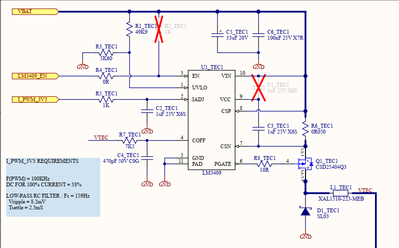
I am using the LM3409 to drive a current controlled device (NOT an LED) with the max output current set to about 4.85A with a 50mOhm sense resistor.  However, I intend to use the IADJ pin to reduce the current dynamically to control the output device.  But for now, I'm just testing the circuit to make sure it is working as expected--and it is not.

The issue is that when the output device is connected (either with the on-board H-Bridge OR done manually) the output current immediately jumps to the limit of the  lab bench supply with programmable current limit.  For now I'm just using a 0.1ohm 10W power resistor to make things easier.

I have scoped out (attached: dark blue is IADJ, light blue is EN) the IADJ pin and EN pin.  I dynamically control both as this is required for the intended device.  You can see that every 1.2 seconds or so I am turning the LM3409 off and the IADJ pin is driving to 0V.  Then, the output h-bridge is switched, the LM3409 is enabled again, then the IADJ pin is ramped up to its maximum (~350mV in this case).  This is all done to reduce thermal stress in the output circuit, though the final application will have much longer periods by about 100x.  I've shortened the time to make testing easier and quicker.  This scope was taken when the output device was removed, so no load.  That also proves out that I'm not getting dead-short of h-bridge FET's.

My understanding is that with IADJ = 350mV the output current should be limited to 0.35/1.24 of the max current set by the sense resistor.  So in this case that would be ~1.4A.  But when I connect the load, I see the power supply hit the current limit with output current up to 5A!  So for some reason the current limit isn't being observed by the LM3409.

I populated C3 because, initially Q1 had a much larger gate capacitance as per the discussion of page 22 of the datasheet.  I haven't updated the schematic to account for that yet, though my understanding is that this would just cause a bit more inductor ripple which is little concern right now.

Any idea on what is going on or how to debug what is going on?

  • So here's a really weird thing: I stopped driving the EN pin so it is just pulled low with a 1K resistor and the same thing happens! How is that possible since the pass FET is controlled by the LM3409 and with it disables the pass FET Q1 should never be turned on.

    I scoped the gate voltage with the input voltage and it looks like the Q1 pass FET gate voltage starts to drop in advance of the voltage collapsing. Why/how is the pass FET gate being driven at all with EN=GND? I also had UVLO setup around 12V and with VBAT=9V input I see the same thing. I tried increasing VBAT to 14V but no difference in behaviour.
  • I've also confirmed that there is a measured 48.8 mOhms across the sense resistor using a relatively accurate, but not calibrated, ohm-meter. I also measured the voltage on both sides of the sense resistor and let the oscilloscope do the math (don't have a floating, diff probe) and I read about 940mV across the sense resistor during the peak current just after it turns on. Again, this happens whether the LM3409 EN pin is GND or 3.3V, which is really weird.

    I suspected my power supply so I used a different supply, without current limit. It's can do 15V 13.5A and it collapses when the output load is connected. So something is definitely not correct with the current limiting.

  • Hello James,

    The initial post with the scope shot I can understand. That is likely just the device going into low power shutdown mode which usually happens in about 10ms of EN being pulled low. That is easy to fix, you can just drive the UVLO pin rather than the EN pin. That will prevent the device from shutting down and IADJ will stay high and VCC will remain alive.

    As for tying EN low and the device is still behaving strangely that sounds like some other issue, maybe noise? These devices can have problems if the DAP is not soldered down properly and/or the layout is poor. Layout is critical in switching regulators and if that is a possible issue I would be happy to check your layout and comment because you are correct, VCC should be 0V with EN held continuously low and since VCC is the gate drive source the FET should have no way to turn on.

    Regards,

    Clint

  • Thanks Clint,

    The first scope shot above is showing how I was controlling the IADJ pin relative to EN pin.  I've since just enabled the device and left it on for now to make things a bit easier.

    I switched to using the actual device I intend (peltier) and that solved the power supply browning out.  I was using a 0.1 ohm resistor before thinking that the current limit of the LM3409 would drive it fine.  But I guess it doesn't like that low of load.  I would have expected it to limit current though and not take down the power supply.

    Switching to the peltier and now the external power supply doesn't collapse.  However, I still see ~4.85A through the Peltier no matter what voltage is on IADJ pin.  I ramp the voltage from 240mV down to 0mV over the course of 10 seconds and I don't see any change in the output current.  Isn't that supposed to be an analog dim pin?

    So I can now see that I hit the limit as based on the sense resistor value -- so that is a step forward.  Now I need to understand why IADJ pin isn't working as I expect it.

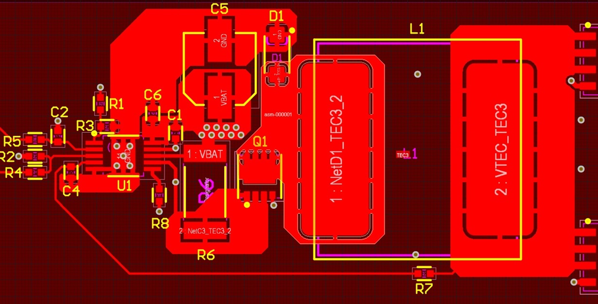
    As for layout, attached is a screen shot.  Pin 1 of the LM3409 (U1) is the top-left as displayed:

    James.

  • Hello James,

    Did you measure the IADJ voltage directly at the pin? Is it possible that it has a solder bridge to another pin? Also, where exactly is C2 grounded? If the voltage directly at the IADJ pin is lowered (below 2.4V) the output current should be lowered.

    I do have some concern about the layout though, other than wondering where C2 is grounded. Your component placement is very good, but I am not sure about the grounding. Having a ground return path that follows the forward switching current paths is crucial. Otherwise you will create large radiating loops that can cause all kinds of issues. Is there a ground plane on another layer? If so I would at a minimum put some vias next to the ground points for C5 and D1. If not I would highly recommend adding a ground plane. If that isn't possible I would at least go ahead and flood the rest of the top plane unused space with ground.

    Regards,

    Clint

  • Thanks for the feedback Clint.

    As for pins shorted together, there are no adjacent pins that have a hard short between them--I measured that.  And visually the soldering looks OK.

    I measured IADJ across C2, which is very close to the device.  So I think that should be fine.

    And yes, I should have mentioned, this is a 4-layer board and there is a solid ground plane underneath this part.  I create a void in the ground plane directly underneath the switching node copper pour on the top layer to reduce its capacitance.  As for return path ground loop, I tried to keep that entirely on the top layer with only 1-connection point to the internal layer.

    Apart from changes to the layout for future designs, do you have any ideas on how to troubleshoot that the output current doesn't appear to be following the voltage on the IADJ pin?  This is functionality that we need--in fact, it was one of the reasons we chose this part over others that only had PWM dimming.

  • One more thing Clint that might help diagnose what is going on. When I have the max current being supplied (because I can't get anything other than max current) and I drive the EN pin low (confirmed with oscilloscope) the output current doesn't change! How is that possible? I don't think this is damage since I've seen both of these symptoms since the beginning of the debugging: EN pin doesn't turn off current and current is always at maximum.

    Any thoughts?
  • I've also noticed that the VCC pin is @ ~8.6V when the EN pin is active (HIGH) and current is flowing as expected. But when the EN pin is driven LOW then VCC floats to 14.5V, where VBAT=15.1V. That looks suspiciously like a diode drop but as you've explained, I expect VCC to become 0V when EN pin is low.

    Does that tell you anything?
  • And the diode D1 is shown backwards in the layout (DOT on the wrong side). It is populated with the cathode connected to the inductor pin. Just to save you some time maybe going down that road.
  • I think I figured it out. Q1 PFET has 4S pins and 3D pins but the symbol has those reversed. So I think the body-diode of the PFET is always ON and current is just flowing through the FET which is why the EN or IADJ pin has any effect. Unfortunately this isn't going to be easy to fix without spinning the board....
  • Hello,

    Yes, I just check your schematic, the MOSFET isn't connected correct.

    Regards,
  • Yep, with FET S+D swapped, the circuit now behaves as expected.