This thread has been locked.

If you have a related question, please click the "Ask a related question" button in the top right corner. The newly created question will be automatically linked to this question.

TPS92515: The LED current calculation which formula to use

Part Number: TPS92515

Hi, there,

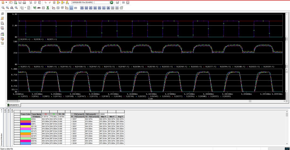
One of our design engineers doesn't understand my simulation result for the schematics in attachment. Per the datasheet dated April 2016-Revised August 2016, in Figure 11 on page 10, The peak Inductor current or the LED current should be equal to the voltage at the IADJ divided by 10 then divided by the Rsense again, the current reading on the L1 should read 17mA per the schematics, but my simulation result shown 858mA reading. Would you please let me know which equation we should be using to verify the simulation result is accurate? I feed 4us period, 2us pulse width of 2.8V PWM signal to the pin PWM of this TPS92515 PSpice model. The Vled has reading of 42V. I put Vin as 48V.

Would you please help me to explain the equation we should be using in the datasheet and plug in the numbers to show the detail? So that I can ensure to our design engineer that the PSpice model that I downloaded from the TI website is the right model to use and the result are trustworthy for our actual production reference. 

Thanks,

Terri

  • Hello Terri,

    Peak current should be 3.5V*(20K/(20K+100K) = 0.583V, 0.583/10 = 0.0583V, 0.0583/(6 ohm//7 ohm)=18 mA peak.

    Off-time is approx 41.5V/26 Kohm = 1.596 mA, I = C * (dv/dt), C=150 pF, dv = 1.0V, I = 1.596 mA, dt = 94 nS.

    Duty cycle = 42V/48V = .875

    On time = 0.875/(1-.875)*94 nS = 658 nS

    Fsw = 1/(94 nS + 658 nS) = 1.33 MHz

    Inductor peak to peak ripple = V = L*(di/dt), V=42V, L=7 uH, dt=94 nS, di=0.564A, this is not possible if the peak is 18 mA so this is running very discontinuous. If the inductor was 1 mH the peak to peak current ripple would be 3.95 mA.

    The datasheet equations are the correct calculations to use. It is a buck converter so general equations such as above work as well. Running high frequency at very low current may be difficult to do. Also, if you are using PWM it won't respond well to high frequency either, 4 uS is 250 KHz pwm rate, it would be better at 250 Hz rate.

    Viadj is set fairly low so the accuracy will not be as good as using higher Viadj.

    Regards,
  •  Irwin,

    Thanks for the detail reply. But the simulation result shows the current and voltage on the LED load response very well to the external PWM control (from V19) and has 858mA current. Please see attachment for the PWM control signal versus the voltage and current on LED load response. I adjusted the VIadj to higher value, and it doesn't impact the current reading that much. I guess I am directly taking the inductor current for the LED current here instead. And this current wave form itself was very steady per the PWM control signal. My question is, should I trust this result from the PSpice simulation tool?

    Thanks,

    Terri

  • Hello Terri,

    Please tell me how there is 858 mA of current with a 6 ohm and 7 ohm current sense resistor?  If Viadj is maximum the peak current threshold is 240 mV.  0.24V/3.23 ohms = 74 mA.  That is as high as the peak current can get with those current sense resistors.

    If the schematic attached is incorrect I cannot help with incorrect information.

    Should you trust the results of the PSpice simulation if the current sense resistors are 6 and 7 ohms and you have 858 mA of current?

    Regards,

  • Terri,

    Looking at your schematic, the off-timer is also referenced to VCC with resistor R8. That will cause a a different off-time than Irwin's calculation. Your timer should only be referenced to VOUT unless you are modulating the load directly with a shunt mosFET in parallel with the load. This configuration could be causing a very short off time. With a short off time and a minimum on-time (see datasheet), it is possible the device is ratcheting the current up uncontrollably when the PWM signal is high. Please look at the datasheet to see the proper connections for the schematic.

    -JP
  • JP,

    Thanks for the reply. I am using external PWM signal, I had to put the R8 in order for this circuit to function in fast on/off time of 4us after I referred to section 8.3.4 in the datasheet. If I changed the Rsense to 0.25ohm, the current output on the series of LEDs became 2A, the LEDs that we chosen normally operate below 1A. And our design limited to certain number of LEDs in series.

    Thanks,

    Terri

  • Terri,

    That resistor (R8 in your case) is only required if you have an external FET (shunt) in parallel with the load.  I don't see that in your schematic.  You definitely should not use that resistor if you are only PWM dimming with the main mosFET of the buck converter (internal to the TPS92515).

    When shunt FET dimming, the second off-timer resistance's purpose is to change the offtime in the fully shunted condition allowing the converter to maintain near constant ripple.  If you are shunt FET dimming, you need to size the resistor different than the standard off-time resistor per the equation (9) in the datasheet.  You should end up with a larger resistance value for R8.

    -JP