This thread has been locked.

If you have a related question, please click the "Ask a related question" button in the top right corner. The newly created question will be automatically linked to this question.

TPS79901DRVR

Hi,
 
I need the layout consideration of SON package.

It is said at the datasheet that the feedback resistors parallel combination should be 250Kohm in order to use the FB capacitors values they suggest.

What does it mean? Parallel resistance or series? At the eval board the parallel resistance is lower than 250Kohm.

Thanks,

Shlomi

  •  

    Hello Shlomi,

    I am not sure what you mean by a "layout consideration"?

    The FB capacitor, Cfb shown in Fig 29 of the data sheet, forms a frequency domain zero with the upper feedback resistor, R1, and a frequency domain pole with the parallel combination of R1 and R2, R1 || R2 in order to add increasing stability to the control loop.  In order that the frequency domain pole should occur at the correct frequency range the capacitance must be within a certain range relative to the resistor values.

    Regards

    Bill

  • Hi Bill,

    At most of TI's LDOs there are layout descriptions below the table of the thermal resistance. These layout suggestions are the conditions in which the thermal resistance was measured.


    I understood these from the datasheet, but the things that I don’t understand are:


    1)    R1 || R2 > 250K ohm? This is a huge resistance. Is this really the demand? At the evaluation board the parallel resistance is much lower than 250K ohm, so again – is there no mistake at the datasheet?

    2)    What is the pole frequency?

     Thanks,

    Shlomi

  • Hi,

    At our application the input voltage is 5V, and the output is 1.5V. When calculating R1 and R2 in order to get the 1.5V output voltage, and R1||R2=250Kohm, I get R1=1.22Mohm, and R2=314Kohm. These values seed high to me (1.22Mohm has a lot of noise, and get close to the opamp input resistance).


    Also, at the eval board the voltage divider wasn't this high.


    What should be the values of the resistors?

    By the way I didn't got answer for my last question. 

    Thanks,

    Shlomi

  • Hello Shlomi,

    You an change the R & C without changing the frequency compensation. Just make maintain a constant product (R*C=constant). 
    For example you can cut the resistances in half then double the capacitance.

    Regards,
    Ron Michallick


  • Hello Ron-san,

    I read the answer of you and Bill-san, bit I can’t understand how to decide the R1, R2 and Cfb for stable and optimal operation.

    Could you please explain the calculation example to decide R1, R2 and Cfb in case of Vin=6V and Vout=3.3V.

    Best Regards.

  • Hello Toshio-san,

    A detailed explanation of the calculation can be found in the following app note:

    http://www.ti.com/lit/an/snva167a/snva167a.pdf

    A quick walk-through is below:

    First you want to find an expression for R1 from the equation Vo = Vref * (1+R1/R2).

    A quick rearrangement of the above formula gives R1 = (Vo/Vref - 1)*R2

    Now substitute this into the equation R1||R2 = 250k, which when solved R1 gives you R1 = 250k * R2/ (R2-250k).

    Now use:

    R1 = (Vo/Vref - 1)*R2 = 250k * R2/ (R2-250k)

    Which solving for R2 = 250k * Vout / (Vout-Vref), and R1 = (Vo/Vref - 1)*R2

    Substituting in the values of Vout = 3.3V, Vref = 1.193V (typical value from the datasheet), we get R2 = 391.6 kohms and R1 = 691.5 kohms.

    Given these, I would pick a value of Cfb of 3pF to 47pF for a quick start-up, although if your layout has quite a bit of parasitic inductance in the path of Cfb I would pick around 500pF to ensure that the parasitic inductance does not overpower the capacitance.


    If you want to design it for fully optimal operation, there is a lot more information involved than just Vin and Vout as you have to place your poles to ensure that your gain is below one when your phase shift starts getting near -180 degrees from your poles and zeroes. A phase margin of around 45 degrees is ideal, which is to say your phase should ideally be around -135 degrees when your gain goes below 1.

    Regards,

    David

  • Hello David-san,


    Thank you for your quick support.

    Please answer additional questions.


    Q1:

    For your calculation result R2 = 391.6 kohms and R1 = 691.5 kohms, I am afraid that current of resistor divider will be close to bias current of FB terminal and it may cause error and high resistance will be weak against EMI.

    Please advise for my above concern.

    And also please advise how to reduce the value of R1 and R2 keeping stable operation.


    Q2:

    I tried to design using Webench and result is follows.

         R2 = 17.4 kohms, R1 = 10 kohms, Cfb=12pF

    2100.WebenchReportsServlet_TPS79901_Vout=3.3V.pdf

    This Webench result does not satisfy R1||R2 = 250k.

    Please advise why Webench output these values.


    Q3:

    I have a project already going with following component and it is difficult stage to change the value of these. So I want to go with following value if possible.

         R2 = 3.3 kohms, R1 = 1.87 kohms, Cfb=33pF, Co = 2.2uF

    Could you please calculate or simulate the crossover frequency and phase margin of above for me to know the stability of my design.


    Best Regards.

  • Hello Toshio-san,

    To answer your questions,

    Q1:
    The values of R1 and R2 give a current of 3.05uA, which as you stated are near the maximum 0.5uA leakage current of the FB pin.

    With worst case conditions, this may present some DC accuracy problems on Vout, however those are the very extremes of the leakage current and the majority of the time the leakage current will be much less, so there will not be an problem. The LDO will be stable though.

    Q2:
    The reason for R1||R2 = 250k is to ensure that the pole and zero due to the Cfb capacitor will be placed for optimal stability with the advised capacitor value ranges for Cfb, Cin, and Cout.
    WebBench relies on other calculations to achieve a stable operational point that are also valid, just not as user friendly.

    Q3:
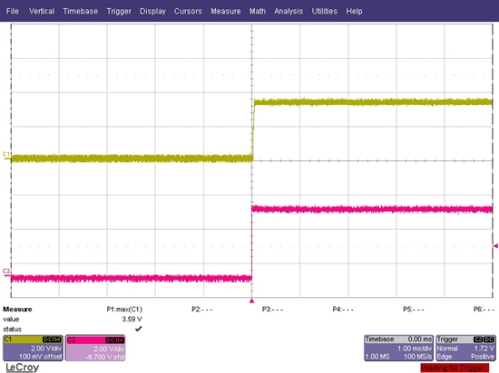
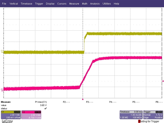
    Based on some quick bench work (scope shots attached of startup waveforms), the LDO is stable at no load and with a load of 170mA with your configuration. The information in my previous post was more about getting an ideal configuration for the LDO with an optimized control loop, which is very time-intensive to do, as you can see from the application note previously posted. Stable operation is a lot easier to verify with one of our EVMs. Another note is that with a 2.7V drop across the LDO, you need to make sure that the PCB design will dissipate the thermals from the LDO if the LDO is operating at a high load. The datasheet has more information on how to ensure the PCB is setup for thermals.

    Yellow is Vout, Pink is EN

    Yellow is Vout, Pink is Vin (the ramp is due to the lab supply being used.


    Regards,
    David

  • Hello David-san,

    Thank you very much for your politeness answer.


    I measured gain and phase of 3.3V and 2.8V output on my real board and results are attached file.

    1588.TPS79901_Gain_Phase.pdf

    Q1:

    Phase margin starts around 20 degree at low frequency.

    Usually it starts with high phase margin at low frequency I believe.

    Could you guess the reason of small phase margin at low frequency?

    Q2:

    Could you give me your comment about stability of 3.3V and 2.8V supply.

    (For example it does not cause problem like oscillation or should be modified because….)


    Best Regards.

  • Hello Toshio-san,

    I'll start with Q2 first - the phase margin looks great for the 2.8V supply and the 3.3V supply for real-world measurements, and you should not see any issues with stability.

    Now to Q1:

    As the gain is decreasing at 40 dB/decade there are 2 dominant poles below 1kHz. I would expect the low frequency phase being near 20 degrees is actually a case of phase wraparound, as you scale is limited to +/-180 degrees. The initial phase should technically start near -180 to -220 degrees with the 2 poles and other nonlinearities, which with phase wraparound would bring it to 20 degrees.

    Regards,

    David

  • Hello David-san,

    Thank you for your answer.

    Please answer my additional question.


    Q1: Low phase margin at low frequency

    I measured with display range 360 degree to -360 degree and results are attached file.

    4643.TPS79901_Gain_Phase_2.pdf

    I believe 20 degree phase margin at low frequency is not caused by wraparound because results are same with original display range (180 degree to -180 degree).

    Could you have additional comment about reason of 20 degree phase margin at low frequency?


    Q2: Stability

    I could not understand the reason of low phase margin at low frequency.

    Could you say that my design is stable in spite of low phase margin at low frequency?


    Best Regards.

  • Hello Toshio-san,

    Measuring gain and phase at 1kHz to 10kHz is difficult on LDO's as a number of different problems can factor in at those low frequencies, from measurement errors to actually causing an oscillation by your measurement, etc. You may still be seeing phase wraparound, but as an artifact of your measurement instrument. You could also be seeing one of a number of other unusual problems that can pop up in a situation like this.


    Your design is stable, and the low frequency information can easily be distorted by a number of factors so you can safely ignore the low frequency phase. The low frequency gain tells you that you have your expected two poles due to the error amplifier and the load pole below 1kHz, which is as expected. The phase that matters is that your phase doesn't cross zero in this case until your gain is below 0dB, and the phase when your gain crosses 0dB. The LDO is stable as the poles are in the expected locations, and your phase margin is 38 degrees at 3.3 Vout, and 90 degrees at 2.8Vout.

    Regards,

    David

  • Hello David-san,

    Thank you for your courteous answer.

    Above questions are from my customer and they understand their regulator is stable.

    Could you please answer following additional question from customer?


    Please let me known the internal circuit of FB terminal.

    Are there any internal pull-up or pull-down register to fix the FB voltage when FB terminal is open or another circuit, or FB is simply connected to input of error amplifier only?

    FB current is +/- 0.5uA so I think there are no internal Pull-up or Pull-down, but I want you to confirm.


    Best Regards.

  • Hello Toshio-san,

    There are no internal pull-ups or pull-downs on the FB terminal for this device, as its expected that the feedback network is connected to the device.

    Regards,

    David

  • Hello David-san,

    Thank you for your quick answer.


    Please advise if only error amplifier input is connected inside the FB terminal or any additional circuit is connected to FB terminal (for example voltage clump, ESD protection circuit etc).

    In case of additional circuit is present, please give me the information of circuit.

    I’m very sorry that I could not ask all questions at a time and bother you.


    Best Regards.

  • Hello David-san,

    Could you answer my question?

    Best Regards.

  • Hello Toshio-san,

    I'm sorry for the delay for my response.

    In the normal operational range there are typically no other active circuits on the FB node of an LDO, unless it has a PG that is referenced from the FB node (the functional block diagram will show this on the LDO's in question).

    Just out of curiosity, why does the customer want this information?

    Regards,

    David

  • Hello David-san,

    Thank your for your answer.

    Customer understands that their regulator is stable but their feedback resistance value is significant different from datasheet so they want to confirm their feedback resistance value doesn’t cause any problem connecting FB internal circuit.

    Best Regards.

  • Toshio-san,

    Thank you for checking with the team here on this.

    Using resistor values that are not listed in the datasheet may cause DC accuracy problems, especially if they are much larger than the values listed in the datasheet.

    Regards,

    David

  • Hello David-san,


    As I reported before, customer understands their regulators are stable from Gain/Phase measurement results.

    But they have to confirm stability based on desk calculation theoretically too, for example simulate Gain/Phase plot and check the phase margin.

    I read AN-1148 and AN-1482 but I can’t calculate the Gain/Phase plot because App. Note explains general case. And Web has only transient model so I can’t use simulation.


    Could you simulate Gain/Phase plot if I provide the customer’s design of TPS79901-Q1?

    Or don’t you have any idea to explain the stability of customer’s design?


    Very Best Regards.

  • Hello David-san,


    Customer requests me additional following information to calculate Gain/Phase plot by themselves.

    Please let me known the Rcomp, Ccomp and error amplifier DC gain of TPS79901-Q1.


    Best Regards.

  • Hi Toshio-san,

    I am not able to disclose those values at this time. The customers design should be stable based on the previous work, and if they are that concerned with proving stability they should stay within datasheet recommendations.

    Regards,

    David