This thread has been locked.

If you have a related question, please click the "Ask a related question" button in the top right corner. The newly created question will be automatically linked to this question.

TPS75005 power-up problem

Other Parts Discussed in Thread: TPS75005, TPS54325

Hello,

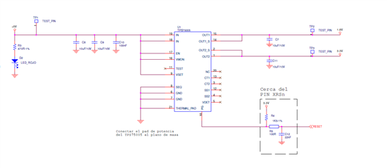
I'm using a TPS75005 (integrated MCU power solution) with a Delfino F28335. I'm using with SEQ=L, VSET=H (1.9V) and i'm not using the third voltage monitor, so EN=VMON=VIN.

This is the scheme:

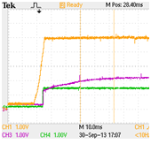
Most of times TPS75005 works fine with these voltages and  times:

CH1 : VIN = 5V , Ramp time = 8ms

CH3: VOUT1(1.9V)

CH4: VOUT2 (3.3V)

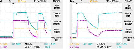
Howerver, we have detected few times that the DSP F28335 doesn't start running, and we found out that VOUT1 is ok but VOUT2 doesn't reach 3.3V. Instead of this, VOUT2 remains at a certain voltage (sometimes around 1.4V and sometimes around 2.2V).The following image is an example of this problem.

It seems like VIN ramp is the same and  VOUT2 has the same load in both cases.

We have around 84uF connected at VOUT2 (distributed in all the PCB), so we know that TPS75005 could be current protected due to this big capacitance, but we think that if this was the case, VOUT2 should return to LDO2 Ramp state, not remaining at some fixed voltage.

Do you have some explanation about this problem? Using the third voltage monitor could be the solution for this?

Thank you very much!

  • Hi Maite,

    I am unable to see your waveforms or schematic.  Could you please try to send them again?

    Very Respectfully,

    Ryan

  • Hi Ryan,

    I send you both images again. Thank you!

    Best regards,

    Maite

  • Hi Maite,

    Thank you for posting both images again.  It looks like your VOUT2 may be being held to a voltage.  Have you checked downstream to see if anything could be holding VOUT2 to a different voltage than 3.3?

    Very Respectfully,

    Ryan

  • Hi Ryan,

    thank you for the answer. I've checked the circuit and it's true that VOUT2 is not 0V when the TPS75005 is not supplied, we have some voltage due to the measurement circuit of our power stage. This is something we will have to check. Anyway, we can isolate this power stage measurement from our DSP circuit board, so this initial voltage of VOUT2 disappears. The problem is the same, sometimes VOUT2 doesn't reache 3.3V.

    We have tried with adding a capacitor in VIN (5V) (470uF)  but the problem still exists. Now we are doing some tests with an external voltage supervisor that enables VIN of the TPS7005 at 4.5V. If it works, we hope that adding the third voltage supervisor of the TPS75005 could be the solution. I will tell you the results.

    Thank you very much.

  • Hi Ryan,

    I have the same problem. And waiting for the solution.

    Thank you very much.

  • Hi Jiang,

    Could you please provide a schematic and waveforms?  These will help in the debugging process.

    Very Respectfully,

    Ryan

  • Hi Ryan,

    during all this time we have tried to improve our design in order to solve the problem with the TPS75005.

    We realized that TPS75005 got blocked by UVLO protection due to all the initial consumption when 3.3V output was enabled. Then, if there is another "enable signal" (+5V > Vthreshold) without OUT1 reaching a value below Vdown 2 (0.3V), TPS75005 remains in a undefined state. The following images show this phenomenon:

    In order to solve this we used the VMON pin according to the datasheet, so OUT1 is enabled around 4.5V, so we try to avoid problems with UVLO because the outputs are enabled at a greater voltage of VIN.

    We redesigned our PCB but thre problem persists and we have a lot of doubts about the good performance of TPS75005. The problem persists and its absolutely arbitrary since we didn't appreciate any difference with VIN voltage ramps when the device starts-up correctly or not.

    We have decided to return to TPS767D301, but we would appreciate some explanation about this problem, and the possibilites to solve it.

    thank you very much.

    Yours sincerely,

    Maite

  • Hi Maite,

    It sounds like you are experiencing a side effect of our power down monitoring.  If both outputs do not go below 0.3V before the start up sequence begins, the device will not start up properly.

    Very Respectfully,

    Ryan

  • Hello,

    I experience the same problem as described - 3.3 V does not ramp up properly. Did anybody find a workaround for this issue?

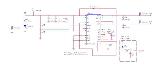
    For further discussion you find my schematics below. My 5 V power supply is created by a TPS54325 step down converter.

    Thank you for any advice!

    Kristin

  • Hi Kristin,

    If this is the same as described, the issue is that the outputs are not going fully to ground before startup. This is required by the device as noted in the datasheet and copied in my post above.

    Please further note that this device is not recommended for new designs. TPS767D318 is recommended for similar functionality.

    Very Respectfully,
    Ryan
  • Hello Ryan,

    thank you for your reply. I have some boards which I soldered the components on myself and some boards which I got fully manufactured. All PCBs are based on the same layout. The only difference I can think of is that the power pad of the TPS75005 is not soldered to the board in my manually factored boards since I cannot reach the pad with the soldering iron. I only seem to face the power up problem with the fully manufactured boards. Could the problem be related to the power pad at all? I am facing the issue 4 out of 5 times when I plug in my fully manufactured board independent of how long it has been unplugged before. Any further advices?

    Kind regards,

    Kristin