This thread has been locked.

If you have a related question, please click the "Ask a related question" button in the top right corner. The newly created question will be automatically linked to this question.

lm317 analysis with additional voltage source on feedback loop

Other Parts Discussed in Thread: LM317, TL2575-ADJ

Hello,

My application involves receiving temperature information from plant to dsp and control the speed of a set of fans according to the temperature.

Voltage on fans should span from 6 to 24V, current lower than 200mA.

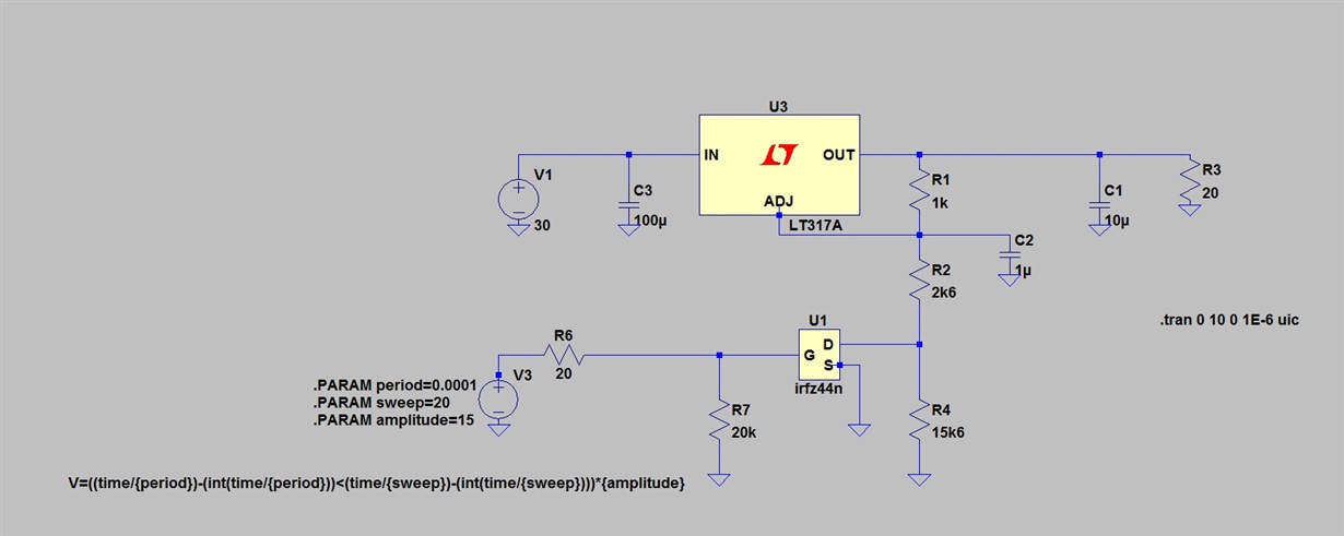
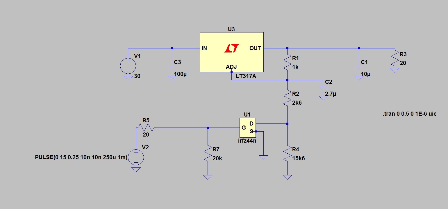
I thought LM317 would be ideal for that, because I can adjust the output voltage Vo using the dsp PWM. So my circuit is:

I chose those R1 and R2 values because, not considering PWM action (e.g, opening MOSFET), Vo is 24V.

Simulations show that for:

PWM >= 20V, LM317 saturates and gives Vo = 28.1V

PWM = 15V, Vo = 23.7V

PWM = 10V, Vo = 18.8V

PWM = 5V, Vo = 13.75V

PWM = 1V, Vo = 9.75V

I find no way to analyse (equate) this circuit. Superimposition theorem doesn't seem very helpful here.

I have seen that the lower R3 makes no difference to the circuit once PWM kicks in.

I have latter found that setting R2 = 1k2 gives me the span I need. In this case, PWM =1V gives Vo = 5V and PWM = 28V obviously saturates Vo = 28.1V.

1) But I can't find an equation for Vo with PWM. How can I equate this circuit when the PWM kicks in?

2) Also, for analysis sake, considering that there is no load connected, I presume that the minimum load current (up to 10 mA) has to flow through the MOSFET and back to VIN supply once PWM kicks in. Is this correct? If yes, power supply has to be able to sink it.

3) Considering the same case above (2), but now load is connected, load current will flow through load and not through MOSFET. Is that right?


Thank you!

  • Thiago,

    To better help you, I have some questions.

    To you want LM317 to pulse width modulate or do you want it to be a linear regulator for 6V to 24V?
    What is the frequency, logic low voltage and logic high voltage, for the PWM signal?

  • Hello Ronald,

    Thanks for chiming in!

    I want LM317 to act as a linear voltage reg., 6V to 24V, controlled by a PWM signal.

    PWM signal characteristics:

    Freq: Just above ultrasonic, about 25kHz.

    0 > Logic low < 0.6V.

    4.3V> Logichigh > 5, pwm source is an usual CMOS uP.

  • I am going to suggest a totally different solution using a simple switching supply better power efficiency and easy implementation.

    Try TL2575-ADJ using bottom schematic in figure 11 of the data sheet.

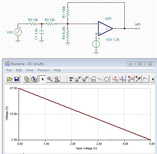
    Replace R1 and R2 with this feedback circuit. (VF1 is VOUT node) (VG1 is your PWM signal) (Inverting input is Feedback pin of TL2575)

    The 1.25V source and op-amp is for DC simulation of the feedback, do NOT add these to TL2575-ADJ.
    With a 0 to 5V input (0% Duty Cycle 0V VOL to 100% Duty Cycle 5V VOH), the output goes from 27.5V to 2.5V
    This is a little bigger than the 6V to 24V request. R1/R3 set the gain. R4 sets the offset voltage.

  • Ronald,

    I'll surely try it. Switching regs. seems a great alternative.

    However, power required (and dissipated) in this application is minimal, maybe 3 or 4 watts total, so efficiency is really not justified. Furthermore, this controller will be close to high EMI sources, so my first thought is that linear regs. are less prone to failure or locks due to interference. I'll test it with TL2575 though.

    Implementation with LM317 seems pretty straight forward too, as simulations have shown. 

    I'd still very much like to know the answers for the questions on first post, if that is possible, specially how to equate lm317 with a voltage source on feedback loop.

    Thank you very much for your support.

    Thiago

  • Thigo,

    I have not tried your circuit but it doesn't work with my understanding of the LM317. For LM317, VOUT is Vadj + 1.25V.
    So I'd expect LM317 out to vary from 8.6V to 13.6V at best.
  • Ronald,

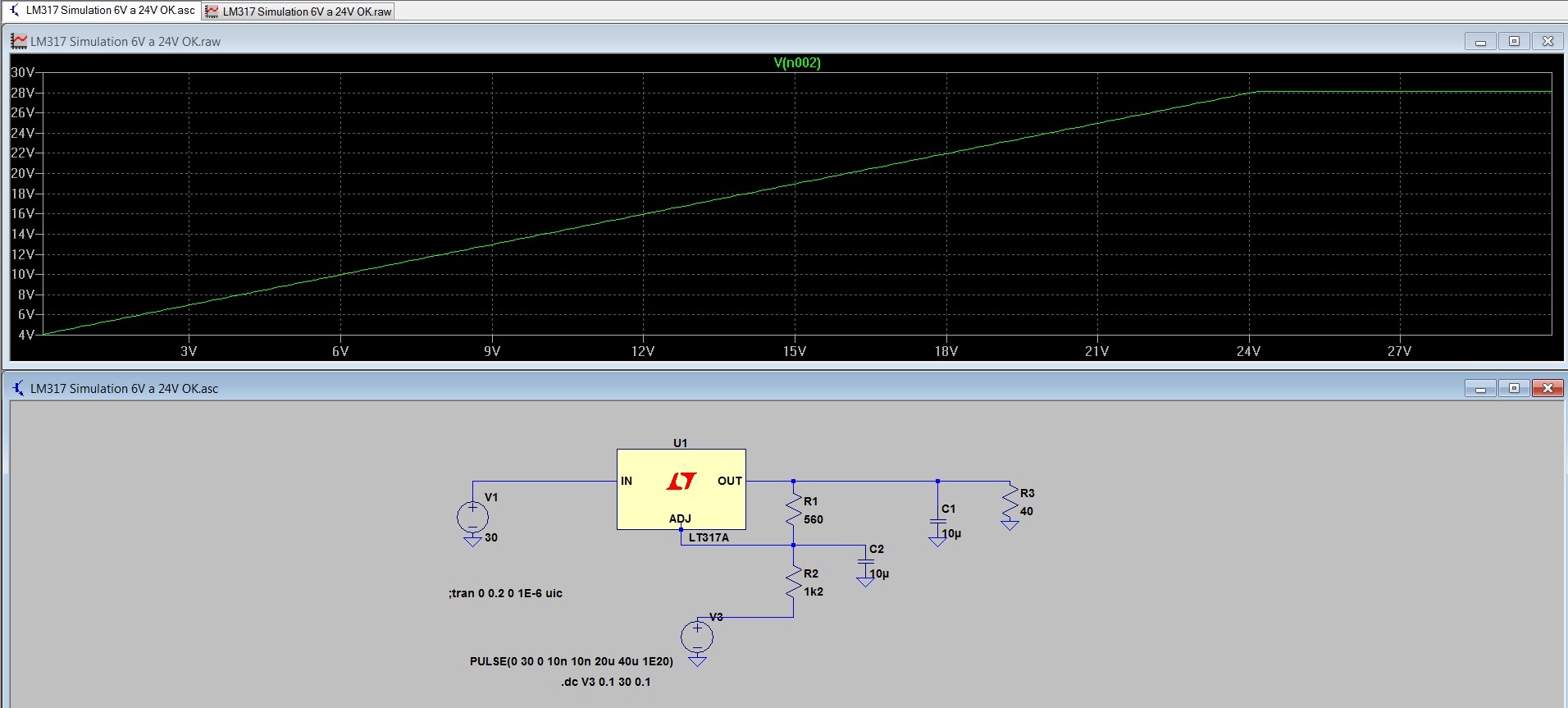
    At least simulation shows it does work, please check DC sweep below.

    In first circuit, MOSFET is switched by cmos pwm, but supplied by VIN, same as LM317 power supply. Equation is simply Vo = Vref * (1 + (R2/R1)) + V2, where V2 is the pwm voltage, in this case.

    Both solutions seem fine, TL2575 requires zener and inductor, whereas LM317 requires an additional MOSFET. Both should do!

    Thank you,

    Thiago

  • Thiago,

    V3 sweep does make sense. Slope of line is 1V/V

    The N channel MOSFET should reduce the PWM signal by Vgs so VIN won't pass through. Also I'm not sure about how LM317 would react to VIN being pulsed to ADJ pin. I would prefer to change PWM to DC before sending to LM317.
  • With 10uF on ADJ pin, the PWM will be RC averaged so the pin will see DC offset from R2 plus the avg PWM, and Vout should be 1.25V above that.

    The fat C2 value calls for the protection diode. The trade-off for the C2 value would be: response time vs ripple.

    I remain confused about the PWM signal characteristics (~0V to ~ 5V) vs the 30V. I don't see how 5V applied to the NMOS gate can drive the Source pin any higher than : 5V - Vgs(th). Unless I missed something here (which is quite possible).

    I did a google search for "LM317 PWM' ... got "About 165,000 results " back.


  • Donald,

    You are right, I made it wrong the first time. A correct idea I later though of is using the FET driven by PWM to provide an alternative path to feedback, reducing effect of R4. If FET is fully and permanently on, R2 termination sees a short, resulting in 4.5V in this case. Vo = 1.25*(1+(R2/R1).

    If FET is open, R2 sees R4 = 15k6 and Vo = 1.25*(1+[(R2+R4)/R1)] = 24V.

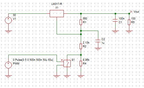
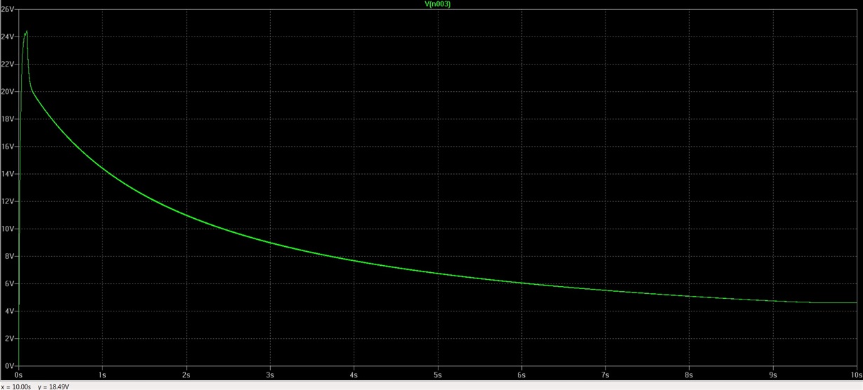
    I've tested with a real circuit and it works like a charm. Simulation below. Note that C2 = 1uF is that low just to haste simulation, since 10uF would take too long to make Vadj stable in a PWM sweep. Real circuit uses 10uF and there is virtually no oscillation seen from LM317. Important to note that duty cycle vs Vout is not linear, specially close to 100% duty cycle. Perhaps a better approach is to design the circuit to a higher upper voltage, so we can avoid this non linear region. V(n003) is Vout.

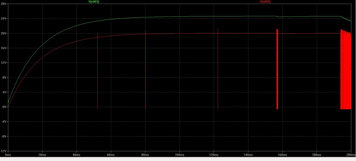
    I just can't explain this weird behavior up to 190ms, please see zoom below. Spurious gate drive, something related to simulation I couldn't figure out what. Changing PWM freq and C2 value also changes the extend of this behavior, but I can't pin point the exact reason. Maybe you can tell me. V(n005) is Vdrain.

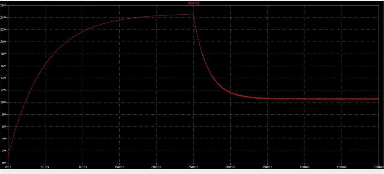
    And here Vgate is pulse, period 1us, 250us on, delayed 250ms: