This thread has been locked.

If you have a related question, please click the "Ask a related question" button in the top right corner. The newly created question will be automatically linked to this question.

TPS7A1601 not working

Dear sir,

We are testing TPS7A1601 for 15V output with following parameters:

Vin= 20V

Cin = Cout = 2.2uF

Feedback resistors:  R1= 12M , R2=1M

At EN (Enable) Pin, I am applying 5V from a battery.

PG, NC, DELAY pins are left floating.

GND is connected to ground of Power supply.

But we are getting only 1.5-2.5V at output.

The EN pin is floating initially, then 5V is applied for some time and then 5V is removed.

However, there is no change in Output due to Enable pin.

The FB pin has 1.2V.

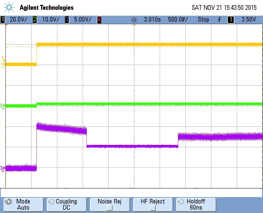
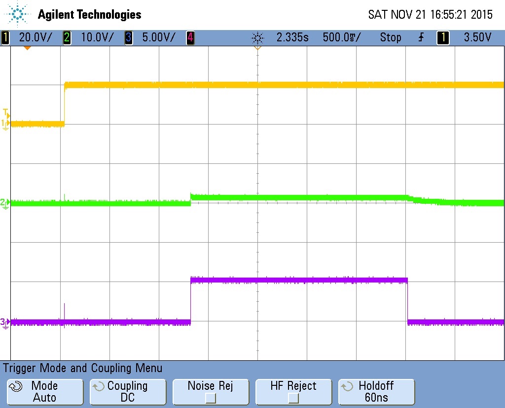
Scope file is attached for your reference.

Channel 1 is Input

Channel 2 is Output

Channel 3 is Enable (It floats from 12- 17V)

Kindly suggest the changes required at your earliest.

Regards,

Gaurav Tarkas

  • Dear Sir,

    I have Pulled down the EN pin (with 2.7K) & checked. There is no change in the output.

    File is attached. 

    Waiting for your suggestions.

    Regards,

    Gaurav Tarkas

  • Hi Gaurav,

    Please allow until the next US business day for a reply.

    Very respectfully,
    Ryan
  • Dear Ryan,

    Still Waiting for your reply.

    Regards,

    Gaurav

  • Hi Gaurav,

    I notice that you are not using the recommended resistors for the 15V output; however, these values should not be yielding the voltage you read.

    There are a few things to check that have caught us in the past. Is your scope correctly recognizing your scope probe as a 10x probe? Are your resistor values the proper resistance?

    Very Respectfully,
    Ryan
  • Dear Ryan,

    1) I had verified the scope readings with a separate multimeter also. Output voltage value was same. So the doubt on probe is eliminated.

        The resistors value are also correct.

    2) I am still getting around 1.19-1.2V on FB pin. Is the feedback loop working OK?

    3) I have also tried connecting a 0.1uF cap on delay pin but there is no change in the output.

       What value should we get on Delay pin?

       I have tried the same on 2-3 PCBs, I am getting same results.

    4) POWER PAD cannot be grounded in this PCB, hence left open. I will modify it in the next layout to be grounded.

        However as there is no load connected in present case, it should not be the reason for this output.

    Plz suggest any corrections.

    Regards,

    Gaurav

  • Hi Gaurav,

    Per the Electrical Characteristics table, you are seeing a valid voltage on the FB pin. Would it be possible to provide a snipit of your layout around the LDO?

    When you say that you tried this on 2-3 PCBs, was this with a new LDO on each PCB? What is your load condition during your tests?

    Very Respectfully,
    Ryan