This thread has been locked.

If you have a related question, please click the "Ask a related question" button in the top right corner. The newly created question will be automatically linked to this question.

TPS61070 Operation

Other Parts Discussed in Thread: TPS61070

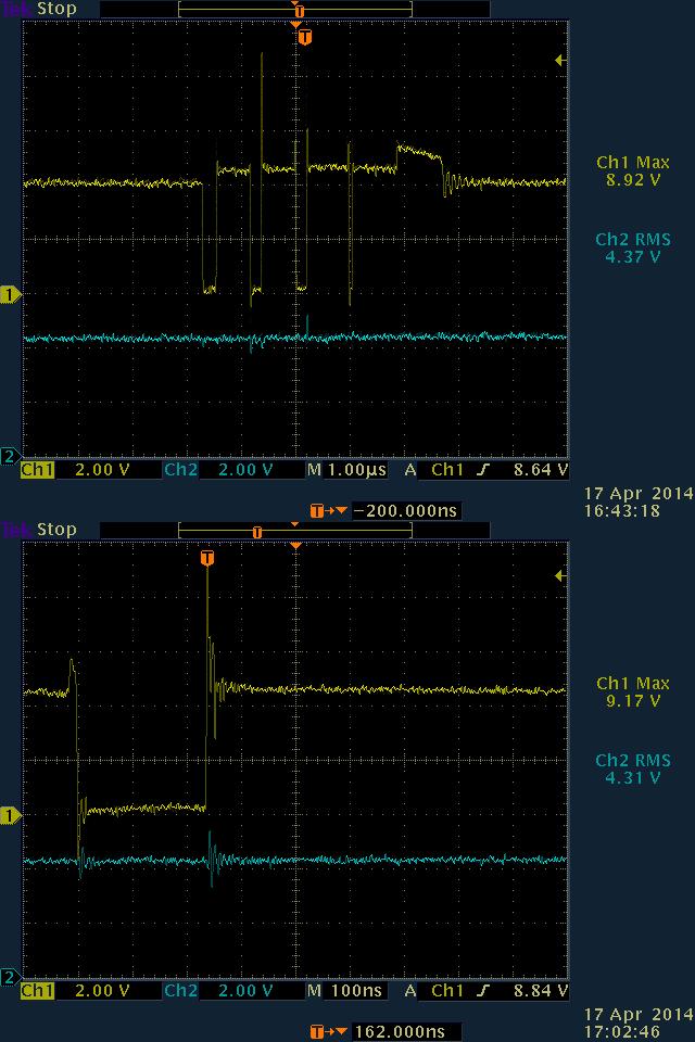
We started testing the TPS61070 kit, added input capacitance of 100uF and output capacitance of 1000uF for battery operation. We found that below 2.4V it was not able to keep us the output voltage of 3.2V whenever transient loads were enabled (simulating radio circuit). Also with a 3.1V input from a power supply – it was not able to provide the 150mA output at 3.2V as indicated in the datasheet.  Is there something we are doing wrong?

-Jason

  • You are likely using way too much output capacitance.  The datasheet says that the Cout should be around 10uF.  The internal compensation is set for this, so by going 100x this value, you are likely causing instability, etc.

    Try testing without the large output cap and see how your results look.

  • Hi! All

    I am using this chip too.

    To using such large capacitor, I guess for transience load.

    If we can't using large value capacitor, what do we do tp improve transience load respond?

    Lewis

  • you can use feedforward to improve the transient performance

  • Jim

    Could you show me a schematic for your suggestion?

  • Here is an AN discussing how to add the feedforward cap.

    http://www.ti.com/lit/an/slva289/slva289.pdf

  • Hello Jim

    Sorry I am busy on another issue before.

    I am using TPS61070 in our many projects.
    It is provided 5V(from Li-iron) for small battery charging & buzzer. The total current consumption is below 300mA(@5V).

    The problem is that the SW pin will become short circuit while power up.

    I have below test.
    1) Increase the capacitor of Vin & Vout. - No improve
    2) Increase the start up delay(to 2s) after power up - no improve
    3) adding small cap.(15pF) between Vout to FB - no improve
    4) try the coil 2.2uH & 10uH - no improve * initially using MURATA LQH32CN4R7M53L

    Below test try to repeat the defect(SW pin short circuit)
    a) enable the chip before power up(Vin) - no damage
    b) let Vout short circuit - no damage
    c) open resistor(between Vout to FB) - no damage
    d) let FB short circuit - no damage

    Shall we make it always power on?
    Is it any power sequence request?

    Our management beginning considers changing another parts to replace it.

    Please help to solve it. At least, I want to clear what going on.

  • Hi Lewis

    the only reason of the SW pin damage is the over voltage stress, most of which result from the bad layout. could you share you schematic an PCB layout please? thanks.

    Jasper li

  • Hi Jasper

    About the over voltage stress to damage SW pin, the chip is mounted in PCB with another circuit.
    And it haven't any connect to let us direct access.
    In board level, we have Li-iron battery(3V-4.2V) only and only this chip has boostor function.
    Base on data sheet the max. level is 7V.

    I don't know why & how the over voltage stress to damage SW pin.

    Please find circuit(attached before) & layout.


    Lewis

  • hi Lewis

    although the DC voltage is only 5V, but the voltage spike at SW pin will higher. if the voltage spike is higher than 7V, there is a risk to damage to the IC. please refer this AN for the root cause and solution of voltag spike of boost converter

    http://www.ti.com/lit/an/slva255/slva255.pdf

    the output capacitor in your PCB is too far away from IC. so  i suspect that the voltage spike in your application is much higher than 7V. please place the capacitor as closed to the IC as possible. you can find PCB layout reference for this device in http://www.ti.com/lit/ug/slvu106/slvu106.pdf and page 16.

    thanks

    Jasper li

  • Jasper

    Thanks for your comment.

    For layout issue, I try adding wire to short the capacitors to pin-2 directly. But no improve.

    And I try adding capacitor(220pF ~ 47000pF) between SW to GND. But the spike level no any change(still higher than 7V)

    BTW, please check with attached picture, there have some abnormal waveform in behind of switching signal.

    Please let me know your comment.


    BR

    Lewis

  •  

    the reason is that the track from IC GND to output capacitor GND is too long, as the red line. please try to place the ouput capacitor above the IC as shown below to double confirm the problem.

    if this work, you can then consider to modify you PCB. you don't need to add snubber if doing good layout. and actually it is very hard to design good snubber, and most of time subber circuit will cause other problem.

  • Hi Jasper

    I have move the output capacitor close to chip(as what you say).
    But the problem doesn’t improve.

    BTW, I try to add 1nF between Vout(pin-5) to FB(pin-4).

    What will be affected of about this change?
    Please let me know your comment.


    BR

    Lewis

  • Lewis

    what is the phenomenon now. does the IC still damage in startup? please share the part number of the cap used. and the waveform of SW pin and output votlage and input voltage.

    the cap from Vout to FB is used to improve the stability of the converter. it should not affect the SW spike if the converter is stable. i stongely suggest that select the feedback resistor  and this cap base on datasheet page 14 (R1 and R2 and CparR1).

    thanks

    Jasper li