This thread has been locked.

If you have a related question, please click the "Ask a related question" button in the top right corner. The newly created question will be automatically linked to this question.

TPS40077 / voltage ripple(rising) after start up

Guru 29690 points
Other Parts Discussed in Thread: TPS40077
Hi Team,
 
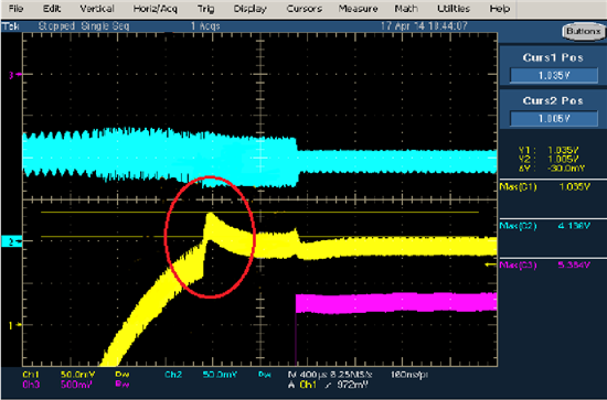
My customer found output voltage ripple(rising) after start up for the file attached.
it seems internally generated and synchronized with PGD pin.
Could you tell me why is it happen?
Is there any workaround to prevent this voltage ripple?
 
It stays about the same in increasing output capacitor.
My customer wouldn't like to change soft start time, so please advise me in other ways if possible.
--------------------------------------
The test condition is following.
VDD=14V
VOUT=1.0V
IOUT=10A
--------------------------------------
 
Best Regards,
Yaita / Japan disty
  • Yaita-san,

    Can you post the schematic? Where is the source of the PGD pullup? How much current does PGD-low draw?

    Have them measure LVBP at the same time to see if that is where the glitch is coming from.

    Regards,

    MC.

  • Martin-san,
     
    Thank you for your prompt reply.
    I confirmed to my customer.
     
    The source of the PGD pullup is Vin for the waveform attached, but the same glitch is occured when PGD is open.
    As a result of pullup, he confirmed the glitch timing is the same timing of PGD.
     
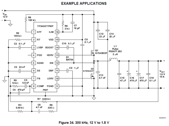
    He said the schematic is almost the same to example application below(datasheet P.34).
     
     
    I also requested LVBP waveform from my customer.
    Your help would be appreciated.
     
    Best Regards,
    Yaita
  • Martin-san,
     
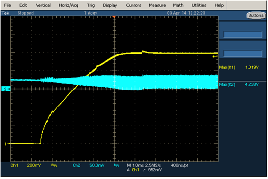
    I received LVBP waveform from my customer.
    ----------------------------------------
    1ch:Vout
    2ch:LVBP(4.2V offset)
    ----------------------------------------
    There seems slightly voltage fluctuation in LVBP.
    Does this fluctuation affect outout voltage?
     
    My customer also said that the glitch level of output vary when changing Low side FET.
    Could you advise me please?
     
    Bets Regards,
    Yaita
  • Yaita-san,

    There is another possibility with the 40077. This device has predictive dead time delay, and when the predictive dead time delay is in effect the dead time is less than about 10nSec. However, when the device is going through soft start, the predictive dead time delay is disabled and the dead time is fixed at about 80nSec.

    When the device is finished soft start, it transitions from fixed dead time to predictive dead time, and that causes a slight change in transfer function. At the transition, the duty cycle will be a bit too high because the pulse width increases by the difference of about 70nSec. At that point the control loop has to re-adjust the duty downwards to compensate.

    Please have them take a high resolution snapshot right as the transition (glitch) occurs. They can probably use the PGD signal as a scope trigger. The picture should be at a timebase that just covers the transition area, and then they can zoom in to the individual cycles to see if they can see the transition in dead time.

    If this proves to be the cause of the bump in the output, they can mitigate the amplitude of the bump with a faster loop compensation, and also higher value output capacitance.

    Regards,

    MC.

  • Martin-san,
     
    Thank you for your support. It's just as you says.
    I received  waveform from my customer and confirmed dead time vary around PGD.
     
    My customer also found that the glitch level becomes lower to change Low Side FET.
    So, if possible, could you advise me how to select Low side FET to lower the glitch?
    I'd like to propose TI FET that suit the spec.
     
    Best Regards,
    Yaita
  • Yaita-san,

    The device uses predictive dead time delay on both edges. In the transition from SW-low to SW-high, the device detects LFET body diode conduction by looking for -VE voltage at SW. On the other edge SW-high to SW-low, the device looks at SW and LDRV and avoids them both being high at the same time.

    For the SW-low to SW-high edge, using an LFET that is slower will help. This is because with a slower LFET, the resulting dead time adjustment from fixed 80nSec to predictive delay will be reduced. For example, it may transition from a fixed 80nSec to a predictive 70nSec, and the delta is small. If the LFET is very fast, it may need to adjust from 80nSec to 10nSec which results in a bigger delta and a bigger volt-second change applied to the choke. Also for the same edge, using an LFET with a lower body diode forward voltage will help, but only a bit. This is because as the device transitions from a fixed 80nSec to "almost no body diode conduction", there are less volt-seconds that are added to the inductor voltage with the loss of the body diode time.

    On the other edge SW-high to SW-low, also using a slower LFET and a slower HFET will help, for the same reasons. The dead time adjustment delta will be smaller. The body diode voltage does not come into play on this edge.

    TI FETs, the NexFETs, will help with the body diode effect. They have a body diode drop that is a bit smaller than other vendors, but again this effect will be minimal.

    NexFETs are not slow, they are extremely fast. So just swapping the FETs out with NexFETs will make the glitch bigger. If they do go with NexFETs, they will need to add small-value (≈ 2 to 10Ω) gate resistors to both FETs to slow them down. But this is actually good because they will have control on the effect by adjusting the gate resistor value to get improvement. If they use inherently slow FETs, they have no control over the phenomenon.

    They should be able to get improvement by designing the loop compensation to be faster, if that is possible. And increasing the output capacitance will also help.

    Regards,

    MC.

  • Hi Martin-san,
     
    Thank you for detailed explanation. I really appreicate for your support.
     
    Please let me ask one more question. 
    My customer found another glitch under the condition of lower Vin(Vin=14V→5.4V).
    ---------------------------------------------------  
    1ch:Vout
    2ch:LVBP
    3ch:PGD
    ---------------------------------------------------  
    Could you advise me why this glitch occures?
    (However the test condition Vin=5.4V is beyond customer's system specification, he would like to know.)
     
    Best Regards,
    Yaita
  • Martin-san,
     
    Is there any method for analyzing this glitch?
    Your support would be appreciated.
     
    Best Regards,
    Yaita
  • Yaita-san,

    Martin is out of the office at the moment, so he has asked me to help you with your issue.


    This does not appear to be a typical start-up, so it will require some additional analysis to determine the likely cause.


    If it's possible to capture this "Glitch" with the following additional waveforms, and hopefully at a higher time-resolution:

    Set One: VOUT, VIN, SS and SW

    Set Two: VOUT, SS, FB and BOOST 

    Please set the scope for 5us / division with a Single Sequence trigger on the VOUT channel rising above 1.02V so that we can check the main control signals that would be affecting the ouptut voltage at this point.  I'm looking for a reason the duty cycle might suddenly change

    In addition, can you check the RT and KFF resistors to see if the part may be operating very near UVLO and VDD is drooping?

  • Hi Peter-san, Martin-san,
     
    Thank you for your kindness.
     
    I checked TPS40077_EVM behavior but couldn't see the same glitch.
    My customer thinks this glitch level depends on external FET.
    I'll check your request with my customer.
     
    Best Regards,
    Yaita