This thread has been locked.

If you have a related question, please click the "Ask a related question" button in the top right corner. The newly created question will be automatically linked to this question.

Reg: LM3488 Boost convertor output oscillation without minimum load

Other Parts Discussed in Thread: LM3488, LM3481, LM3478

Hi, 

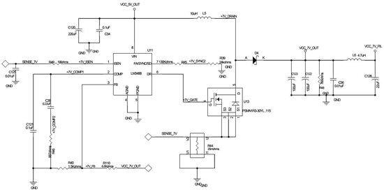
I am using LM3488 in boost configuration for generating 7V from 5V.

I have implemented the schematic from the WEBENCH Design Report.

During testing a 50Hz oscillation with 300mV peak to peak voltage is observed in the 7V output with 10mA minimum load. 

When the load increased to 30mA, the output becomes stable with ripple less than 50mV.

The schematics of the circuit is also attached.

Is there any solution available to reduce ripple with 10mA or less load.

  • Hi,

    Can you see the oscillation waveform? Is the 300mV ripple at 50Hz a sawtooth waveform?

    Best regards,
    Tommy

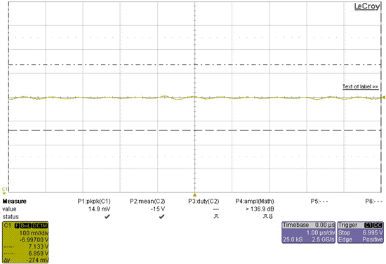
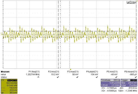
  • These are the output ripple with 10mA & 30mA load.

    Please note, with 30mA load the output ripple reduced to 15mV from 276mV.

    Sagar

  • Hi Sagar,

    You are hitting the minimum on-time of the part at low load (sounds like at less than 30mA), this causes the voltage on the output to increase until it hits Over Voltage Protection, it then turns off until it goes back below the regulating voltage, this is why you see the sawtooth.

    Because of this operation the part will always have a minimum load before OVP is reached.
    You can sneak around this in a couple of ways:
    You could look at the LM3481, which is a very similar part and has a smaller min-On-Time (250ns instead of 325ns).
    You can increase you inductance which will decrease the power transfer every switching cycle at min-OnTime effectively lowering the min Load needed to stay out of OVP, but this will also bring in the RHPZ so you might need to adjust the compensation a little.
    And the easiest way, but most inefficient is to have a dummy load on the output so you never actually go under you min load. You could decrease the feedback resistors while keeping the same ratio to do this and you can also feed Vin from Vout so the IC's current draw is used to load the output using diodes from both your actual source and your Vout to the IC vin cap (actually the second way isn't inefficient but only gives you around 3mA extra Load).

    Best regards,

    Tommy

  • Hi Tommy,


    Here the convertor switching frequency is 130KHz and the output oscillation frequency is 50Hz.

    If there is any problem with the minimum load, i think the ripple should  be in the switching frequency(130KHz) itself.

    The changes in simulation and actual component values are,

    Part                        Simulation            Actual

    Inductor                   7.8uH                    10uH

    Switching Freq        184KHz                130KHz


    Regards

    Sagar C S

  • Hi Tommy,


    I have probed the gate signal and found that the pulse train is not continuous with 10mA load (ie, after 500 pulses, approx 50us off period).

    Also the pulse on time is close to 500ns with 10mA load.

    With additional 14 mA load, the output is stable with continuous gate pulse (pulse on time almost 500ns).

    I will increase the inductor value and check again (as i cannot cut the tracks for changing the supply to IC).

    Please explain how the gate on time is limited (as you said about OVP) or provide any application note.

    Regards,

    Sagar C S

  • Hi Tommy,


    I have increased the inductor value from 10uH to 22uH.

    With the change, the output is stable with ripple come down to around 100mV.

    With a load of 2A, the ripple at the LC filter output is not exceeding 200mV.

    Best Regards,

    Sagar C S

  • Hi Sagar,

    Sorry for the delay, I've been out of office.

    For min on time and OVP characterstics check the datasheet. The electrical characterstics show these parameters. For a detailed description of the OVP I'd look at the LM3478 datasheet, page 9. The LM3478 is pin pin the same as the LM3488 except it doesn't have the frequency sync option.

    Min On-Time is the smallest amount of time the Gate drive signal for the FET can turn on for, which means for a given Frequency you have a minimum duty cycle. At low load when you hit min On-Time, the part continues to switch with this minimum duty cycle; during this time each switching cycle dumps a little more current than needed on the output cap. This then slowly builds the output voltage. When the Output voltage exceeds OVP (or actually the feedback pin voltage does), the part stops switching until the load drains the excess current and the voltage goes under another threshold limit set at the FB pin (a little under the regulating voltage). This is why you see the non continuous pulse train. This is also why the oscillation is not at the switching frequency. The sawtooth frequency you see will be determined by the load current, the inductance, the output cap, the min on-time and the OVP limits of the IC.


    The datasheet lists OVP for this device at 50mV above regulation, it also adds 10mV that the part must go under regulation to turn back on, so 60mV of swing at the FB pin during OVP. Since this is at the Feedback pin its reflected to the actual output by the feedback resistor ratio, which turns 7V out to 1.26V at FB, or in effect multiplies this ripple by 5.5 so 5.5*60mV means you would see around 330mV ripple at you VCC_7V_OUT and less on the filter output (you were seeing 270mV right?)

    So your inductance change helped the min load, but introduced that higher frequency ringing?

    Best regards,

    Tommy