This thread has been locked.

If you have a related question, please click the "Ask a related question" button in the top right corner. The newly created question will be automatically linked to this question.

LMR12010 ripple problems

Other Parts Discussed in Thread: LMR12010

Hello,

I have problems using LMR12010. It's very simple step down application from 10Vdc input to 3.6V output.

I followed app note for LM12010 with input capacitors, output capacitors and other recommended parts.

Evrything works fine when I have at least 100 ohm load (resistive). When I increase the load (1kohm) output 

voltage becomes unstable (looks like pumping output signal from approx 3.2V to 3.9V). This saw shape signal

(fast rise and slow drop) has frequency dependent on load. It is like 30Hz at 150ohm load and rises when 

I increase load resistance. Amplitude of this ripple is not affected by a load. Only frequency is affected.

I use 1000uF as a bulk input capacitor plus 100n and 10uF ceramic. Inductor is 15mH tiny power inductor, output

capacitors are again 100n and 10uF caramic plus 220uF ELCO. FB resistors are 12k and 47k.

Any idea what might be wrong?

Thanks in advance

Humar J

  • Are you using a 15 milli henry inductor or is that a typo?  If you are try substituting a 15 micro henry inductor and recheck the design.


    Regards,

    Marc

  • Hi Marc,

    Yes, it was a typo. I'm actually using 15 micro inductor.

    I did some extra measurements and I belive, that this component is just didn't ment to be

    used with low loads. I noticed that it obviously works in two modes. When I connect with a scope

    to a point where current is injected to inductor it is clearly seen how regulation is done with different

    duty cycles. This is normal mode

    When load is decresed at first duty cycle is also reduced. But at some point (when load is approx.

    100ohm @ 3.6V) output starts jumping. It looks like minimum time FET is opened is already too much

    energy injected into inductor. So the voltage rises a few 100mV over defined limit.

    Then there is longer pause in current bursts and when voltage drops below

    predefined threshold (this time is dependent on output capacitor)  FET opens again for a minimum time periode

    voltage rises over and so on. The result is low frequency ripple.

    There is no info in datasheet about minimum duty cycle for driving output FET.

    regards

    Janez

  • Hi Marc,

    Any further suggestions regarding explained problem?

    I already posted more comprehensive description.

    regards

    Janez Humar

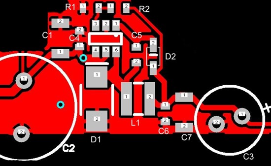
  • Can you post your layout?  Sometimes noise from the layout can cause issues.


    Regards,

    Marc

  • Thinking about it. It sounds like you are not fulling charging your boot capacitor.  This is more of a problem at light load currents and higher output voltages, but if the boot voltage is not high enough then it could be seen at 3.6Vout.  What voltage are you using to supply the boot voltage?

    Try connecting a schotcky diode from 5V to the boot cap and see if the problem goes away.

    Regards,

    Marc

  • Hi Marc,

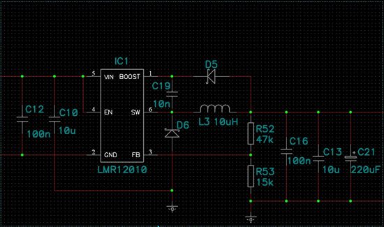
    As you see in schematic, I'm using output voltage to drive Vboost. In datasheet it is written that  "Vboost needs to be at least 1.6V greater then Vsw". But since in my case voltage for Vboost is actually derived from Vsw it is not possible to acheive this requirement (Vsw > Vboost + 1.6V) unless there is some sort of charge pump with boost capacitor.

    In datasheet it is written:

    An alternate method for charging CBOOST is to connect D2 to the output as shown in Figure 22. The output
    voltage should be between 2.5V and 5.5V, so that proper gate voltage will be applied to the internal switch. In
    this circuit, CBOOST provides a gate drive voltage that is slightly less than VOUT.

    I have done exactly this and it does what I desribed (ripple).Then I tried to feed voltage to Vboost from Vin (8V) through schottky diode and then it works perfectly. But that means that method to derive Vboost from output voltage is not operational?

    There is another problem to it. Big advantage of LMR12010 is wide input voltage range. But if I use

    Vin as an input to Vboost I need to take care of condition (Vboost-Vsw < 5.5V). Therefore I need to 

    install extra zenner diode. My input voltage can vary from cca. 5V up to cca 10V. 

    Thank you and kind regards

    Janez

  • There are a couple things we can try, in this order.

    1) Replace D2 with an larger schottky to try and lower the forward drop.  Try using the same one you are using for D1 just as an experiment.  This will help to raise the voltage charging the boot pin.

    2) Try a 6.8uH inductor for L1.  The increased current ripple can sometime give the boot capacitor more time to charge in light load.

    3) Increase the boot capacitor to 22-47nF.  THe extra capacitance might give us a little more charge.

    4)  Lower the values of feedback resistors R1 and R2 by a factor or ten so that there is always a small load.  This helps to keep the boot voltage charged.

    5)  Last resort use a zener from vin to derive 5.1V.

    Not related to the light load issue.  You should probably rotate C1 and C4 so that their grounds are next to the ground of D1.  This will help to reduce switching noise in your layout and you will find that the high frequency noise on the output voltage and input voltage is reduced.