This thread has been locked.

If you have a related question, please click the "Ask a related question" button in the top right corner. The newly created question will be automatically linked to this question.

TPS54260QDGQRQ1 PWRGD Ripple

Other Parts Discussed in Thread: TPS54260


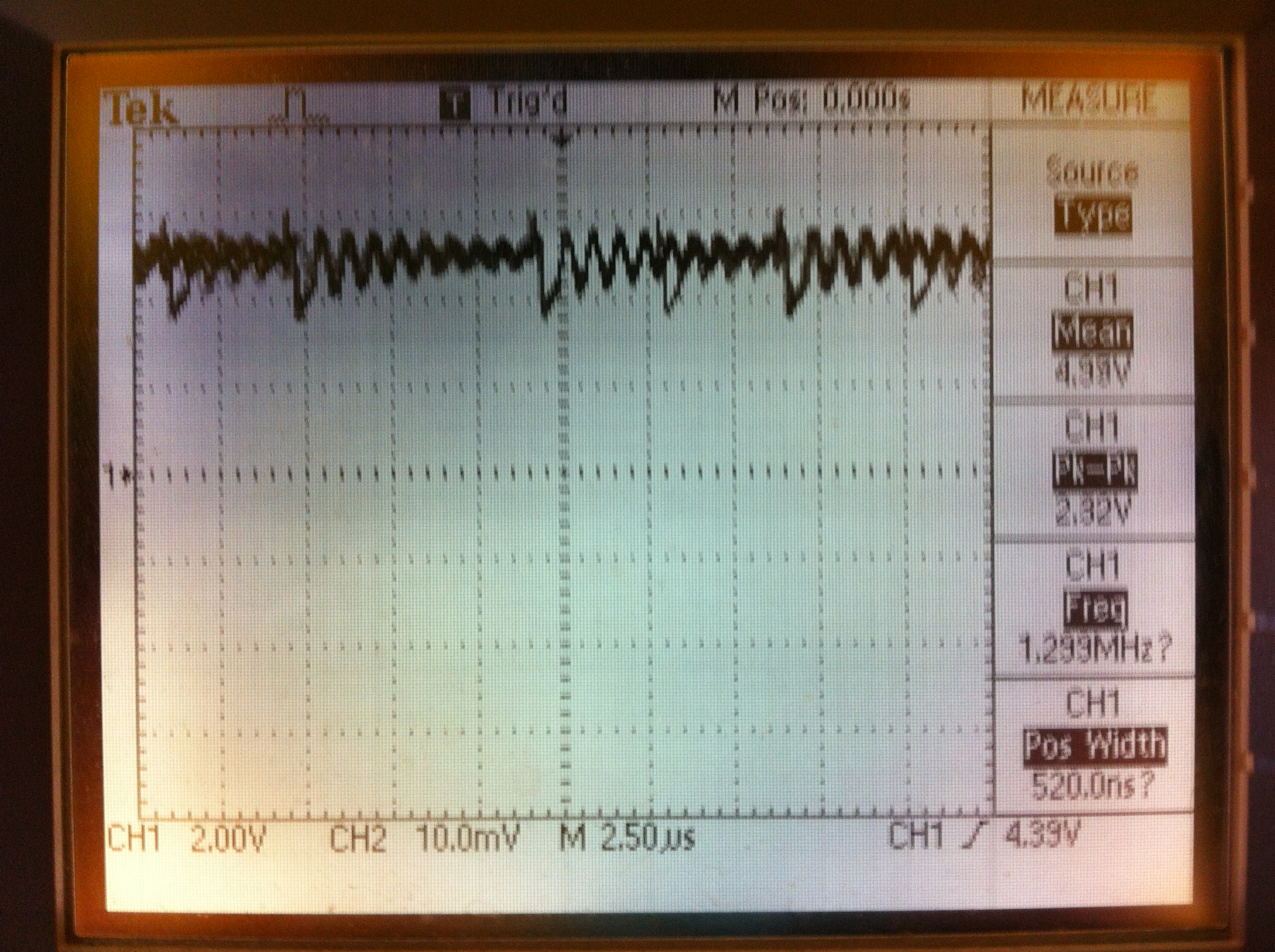
Have problems with ripple in PWRGD pin that causes uC to reset at higher input voltages (>16V).  

The circuit uses a PIC processor internal pull-up to 5 volt. This pull-up is approx. 35k, recommended pull-up resistor from data sheet is 1 – 100K.

Images are for 14volt in 0A load and 2.5A, ripple is not affected by load 0.1 – 2,5A only input voltage.

Is this ripple normal?

Regards


Stefan

  • I don't recall ever seeing that type of ripple on PWRGD.  Is the ripple at your switching frequency?

  • Yes, it is the switching frequency. Connector is only for programming uC. PCB layout between uC and PWRGD pin colored blue.

    Missed the images..


  • Are you going to post the layout?

  • If it can be of any help John. So did I found an old post with similar problem but other Buck Converter. We have the same ripple wave form but I have higher amplitude.

    http://e2e.ti.com/support/power_management/non-isolated_dcdc/f/196/t/226005.aspx

    Regards

    Stefan

  • Added a 22k pull-up “externally” slightly less amplitude at 14V but at ~27V in uC still resets.

    This can’t be normal, can the Buck Converter be damaged?

    Regards

  • Could not resist in some experimenting….

    Made a destructive test and connected a 0.1uF and a 22k between PWRGD and 5V. With 14 volt in PWRGD was quite stable on the oscilloscope. But when I increased to 30V there was death smoke from TPS54260….  

    I’m thinking, for some reason PWRGD is grounded (many mA) by the buck converter at switching frequency and this is not high impedance transients generated from poor PCB layout.   

    Any suggestion why this happen?

    Regads Stefan

  • I have seen some large ripple caused by placement of the PWRGD pull up resistor in the past. The best thing to do is reduced the pull up resistance value to the minimum. Also a small capacitor of maybe 100pF could be placed near the microcontroller to filter out the switching noise to avoid false resets.

    It seems like 4 of the images didn't come through on your post but I can see some of the layout. Where is the PWRGD pull up resistor placed?

    Is U201 the TPS24260? If so and if I'm looking at the layout correctly it seems like the switching node is extremely large. It is recommended to keep this as small as possible to limit any capacitive coupling due to the high dv/dt signal located on the node. It should also be kept wide to limit inductance in the path since it carries the switching current.

  • Adding a new print screen for top copper that also show paste mask so it is clearer to see component footprint.


    Adding print screen with bottom paste mask, output inductor 7443634700 (L203) are the two lager square solder pads I bottom of picture.

    The catch diode (D206) D-PAK anode pins are placed on both side of TPS54260 (U201) and the output inductor (shielded) is on the bottom side of PCB just under TPS54260 together with output capacitors (C213 and C214).

    What part of the switching node is long?


    There is no external pull-up resistor, originally I use the internal pull-up in the uC PIC16F1825 (U203).

    For testing I added a 22K resistor in parallel with uC this would be approx. 13.5k pull-up. (TPS54260 datasheet recommends 1 – 100k) NO CHANGE/MINIMAL CHANGE in ripple with the extra resistor.

    Do you think it is high impedance noise generated by switching node?

    That was also my thought so a tested with a filter capacitor but the current true PWRGD pin was so much that smoke coming and a burned spot on top of TPS54260, it is now dead.  (I have more).

     I’m not so sure that it is noise, but you may have good comments on the PCB traces and component placements, as it hopefully clearer with the added images.

    I will try to filter with a 100pF and use 1k pull-up resistor.  

  • A couple of comments after reviewing the new screenshots. There are definitely a couple things in this layout which are not ideal and could contribute to noise on the PWRGD pin. The EVM layout could be used as a reference for these recommendations.

    1. It would be better to move the diode down so that all ground connections are made on one side of the TPS54260 IC. In other words, keep the diode on the pin 10/pin 1 side of the IC for short return to the input capacitor. With the placement now some of the high di/dt switching currents may flow underneath the IC, right next to the PWRGD pin and some of the other noise sensitive analog control circuits. This could be a source of noise to the PWRGD pin. You might be able to test this out on your current PCB. Using a diode with a different package, maybe an SMB package, might make this easier.
    2. There is a lot of unnecessary PH copper. I recommend removing all of the copper that isn't used to connect the PH pin, diode and inductor. Have a short and wide direct connection between the PH pin, diode and inductor.

    I haven't had issues using a small capacitor from PWRGD to GND, up to 1000pF. I recommend placing this capacitor near the uC pin that is inputting this signal.