Hello all,
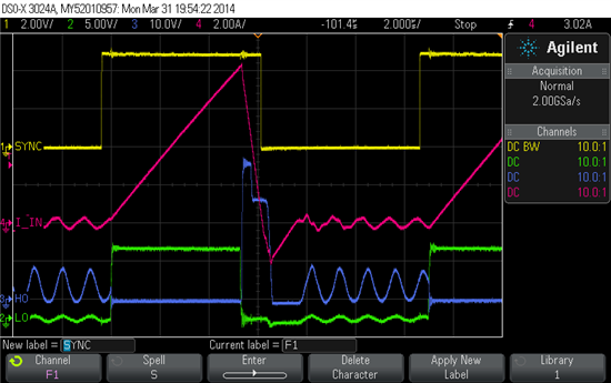
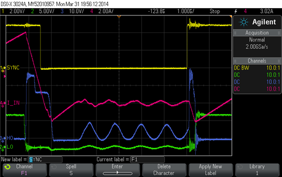
I hope someone can help me with problem on LM5122 syncro FET control pulses. I have attached 2 pictures related to problem described below, there is normal cycle, and cycle where syncro FET control is activated incorrectly in the end of cycle.
Idea is to have 2 interleaved PSUs which are controlled by 75kHz and 50% duty cycle control signal which is directly connected to other PSU and inverted for the other. PSUs dont have RT & CT components and are not configured for free running (master2 mode is used). LM5122 is also configured for diode emulation mode. Vin = 3.5 and Vout = 24V, Inductor current is sensed over 3mΩ current sense resistor, there is filtering of 470Ω in series on both CSP & CSN pins and 100pF capacitor between then next to LM5122 pins.
In both pictures scope channels are:
- buffered digital 0…5V sync pulse with 75kHz frequency and about 50% pulse width, (yellow trace)
- LO, main FET gate control signal. (green trace)
- HI, syncro FET gate control signal. This channel is referred to GND so it is actually HO+SW (blue trace)
- Inductor current, actually only 50% of real current since inductor is made from 2 parallel wires and only 1 fit through current probe (red trace)
This problem seems to occur only if inductor current, or more specifically in this case current sense voltage is above 0-current level when new synchronization pulse comes. (caused by “ringing” voltage on main FET drain)
Is this control error only caused by voltage level on current sense pin when new cycle starts or can other things contribute to this, example: slope compensation, synchronization frequency and pulse width or something else…


