This thread has been locked.

If you have a related question, please click the "Ask a related question" button in the top right corner. The newly created question will be automatically linked to this question.

LM5116 design Questions.

Other Parts Discussed in Thread: LM5116

Im attempting to make a high efficiency buck regulator, as my input power is restricted and i don't want to waste it, and due to packaging requirements getting rid of heat will be an issue as well.    I'm looking at using the LM5116, which on paper will give me efficencys that are suitable.

I have a question about using an external bias voltage.      In the TI eval kit for this chip, it shows the output ( 5V ) tied back to VCCX via a 1R resistor.      The documentation for the IC, its shown directly connected, to the output.     

My output will be 5V.    In my design i've decided to provision a resistor, but if it turns out its not needed, i'll install a 0R0 jumper.

Can anyone explain what the resitor might have been for?

  • Hi 

    The purpose of the resistor connecting Vout to VCCX is to form a RC filter. VCC/VCC is required to be as stable as possible.

    Using 1 ~ 3 ohm resistor is a good compromise between 'good filtering' and 'small voltage drop across the resistor'.  

    Regards,

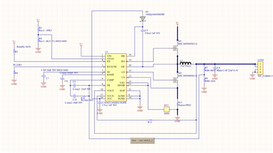
  • Thanks Eric , below is the schematic of what i'm building.    A compromise of inductor size / FET selection etc etc.  The output is designed to be 5.0V.    R12 is my placeholder resistor which i'd not quite decided what to do with.      

    I couldn't find any referencing to filtering VCCX,   I'm assuming this is forming a filter with the capacitor on VCC?     

    Could you elaborate any further on this..


  • Hi 

    R12 and Cvccx capacitor forms a RC filter. 

    Here are some comments ;

    - Please populate VCCX capacitor close to the IC. 

    - Please populate hiccup capacitor from UVLO to ground if needed. 

    - Double check your Ccomp1 and Ccomp2. 

    Regards,

  • Thanks Eric, i had omitted the Vcxx cap. The Datasheet is very 'light' on the Vccx use.  A short application note for this would be really helpful.     I'd love to know what kind of  Pd I will save by using VCCx.. 

    I've also included a hiccup cap as suggested,  If i don't need it, can simply leave it off, there was enough pcb space.

    Why do you suggest i need to change my Comp1 ( 22nF ) and CComp2 ( 18pf ) these values were generated by the TI workbench.

  • Hi 

    I see 22nF is placed in between FB and COMP and 18pF is connected from COMP to Rcomp in your schematic. 

    Usually, the capacitor which is placed in between FB and COMP is in pF range and the capacitor which is connected in series with Rcomp resistor is in nF range

    Regards,

  • Thanks for spotting that.     I had transposed them in the schematics,    Forutnatly they are the same size physically, so swapping them around is no problem.   PCB is now ordered.