This thread has been locked.

If you have a related question, please click the "Ask a related question" button in the top right corner. The newly created question will be automatically linked to this question.

TPS6122 voltage drop issue

Other Parts Discussed in Thread: TPS61222

Hi,

I'm trying to generate a 5Volts power supply from 3.7Volts LIIO battery by using the Booster TPS6122 http://www.ti.com/lit/ds/symlink/tps61220.pdf

obtained result:

- without load: I have Vout=5Volts

- ISSUE: when the circuit is loaded (10mA and more) the Vout voltage drops (from 5Volts to less than 4Volts).

I used the circuit as indicated in datasheet:

have you any idea why it doesn't work correctly ! 

  • so you are using TPS61222.

    over current limit of this device is triggered, maybe because inductor saturation or input voltage too low. could you share the voltage waveform of Vin pin, Vout pin, L (SW) pin, and also the part number of the inductor and your PCB layout.

    thanks

    Jasper Li

  • I am using TPS6122 for exact same purpose Lithium ION battery (3 - 4.2v) input and 5V output.

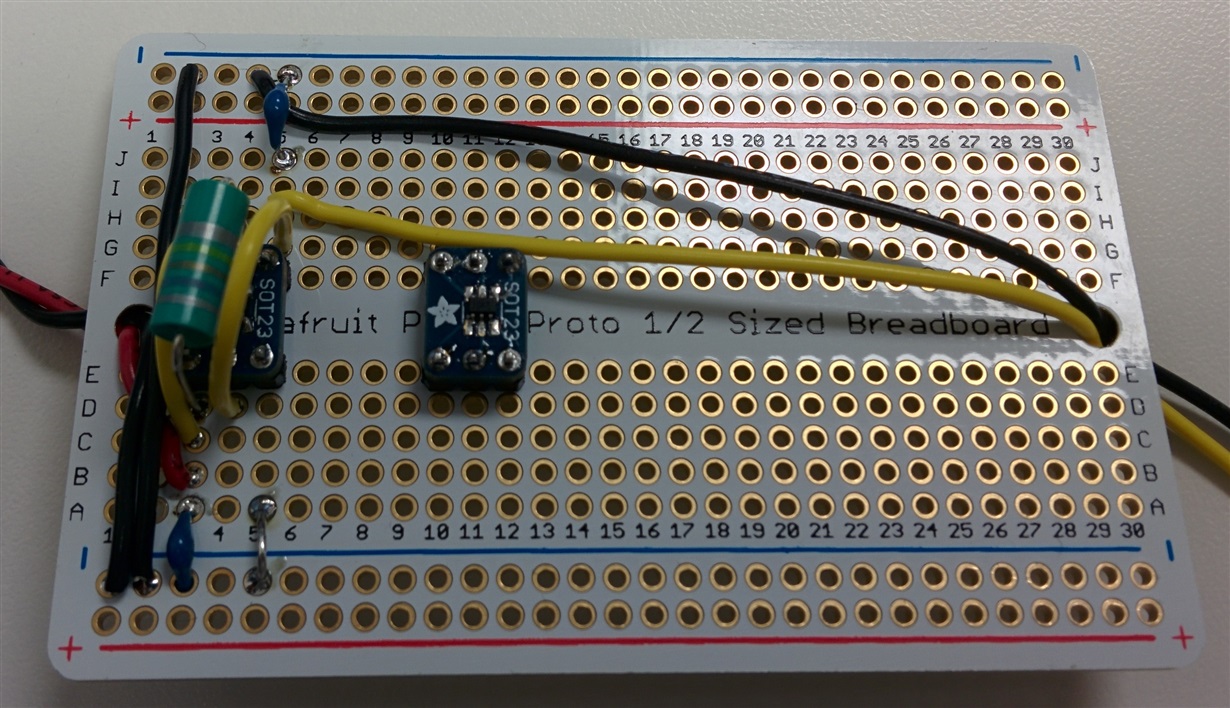
    I am using a (Part No: 541-1541-ND Description: FIXED IND 4.7UH 380MA 550 mOHM) fixed inductor on a general purpose PCB (attached pic) which has a layout like a breadboard. 

      The actual chip is under the inductor. one on the side is just a representation. 

    My problem is similar a voltage drop at output from 5v to 3.8 when i connect the load which will draw 30mA max (Powering an AD7730 just the analog 5v section which is abs max rated at 30mA, tipical 10/15mA depending on the usage) Any help will be appreciated. I am also using 10uF capacitors at the IP and OP as recommended on the datasheet. 

      Signal on L with no load (output is 5.04v, Input voltage 3.7v)

     Signal on L with a lode of 1.5k (output voltage is 3.5v, Input voltage 3.7v and draws 270mA of current at VIN)

     Signal on VOUT pin with a load of 1.5k 

    With no load the signal is clean on the VOUT (didn't notice any noise)

    No change in VIN voltage for both with Load and no load condition. 

  • Kaushik Ray

    the PCB layout is very important for the normal operation of switching power device. the output capacitor should be as closed to the IC as possible. otherwise you observed unexpected behavior.

    i would suggest you to apply an TPS61220EVM or build a real PCB following the suggestion in datasheet and EVM user guide.

    thanks
    Jasper Li
  • Thanx Jasper for the reply i will try some other options before i go to TPS61220EVM. I am a hobby electronics user so i dont really want to spend on a PCB design until i finish my whole project.
  • Was Not able to make this work on a general purpose PCB but i am sure it will work with a right PCB. I moved to LTC3525-5 works great on a General purpose PCB. Using a snubber I get a really clean signal :)