This thread has been locked.

If you have a related question, please click the "Ask a related question" button in the top right corner. The newly created question will be automatically linked to this question.

LM2586 Soft Start

Other Parts Discussed in Thread: LM2586

Hi,

I ask for SOFT-START block of LM2586.

From the block diagram of LM2586, I'm understanding that SOFT-START block controls the error amp.

How does SOFT-START block control the error amp?

I can't find the description of SOFT-START from the datasheet.

Thanks and Regards,

Kuramochi

  • Hi,
    I changed question.
    I'd appreciate comments.

    Thanks,
    Kuramochi
  • When the device is first started-up, the error amplifier is disconnected and an 11uA (typ) current source is connected to the output of the error amplifer. This current slowly charges the external compensation capacitor connected to the COMP pin. The voltage on the COMP pin slowly rises, causeing the duty cycle and the inductor current to increase. This controls the inrush current. The output voltage is ramping up at this time as well. When the output voltage reaches about 15% above the regulation point, the current source is turned off and the error amplifier is turned on. Normal regulation can no occur. UVLO, TSD or ON/OFF will reset soft-start and discharge the compensation capacitor.
    FD
  • FD-san

    Thank you for your reply.

    I understood.

    LM2586 has a problem on the boost circuit.

    The output voltage is 15V.

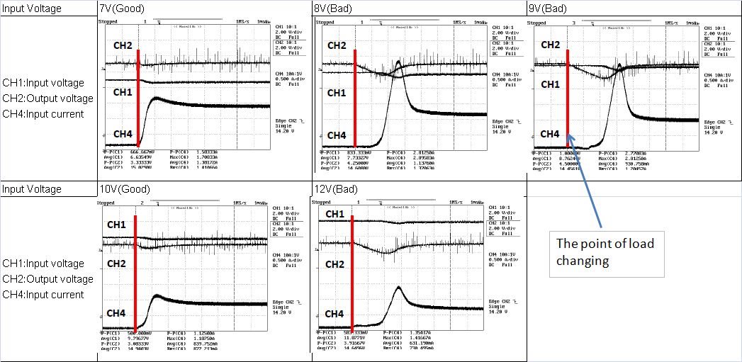
    The problem is that load response character is bad for particular input voltage.

    The load is changed from 0A(no load) to 400mA.

    I attach waves and the circuit.

    I'm sorry that Japanese is included.

    What is the cause of this problem?

    I think that soft-start may malfunction.

    Please let me know any question.

    Thanks and Regards,

    Kuramochi

  • I do not think it is the soft-start. It may be that the compensation needs to be adjusted. Or you may need more input capacitor.
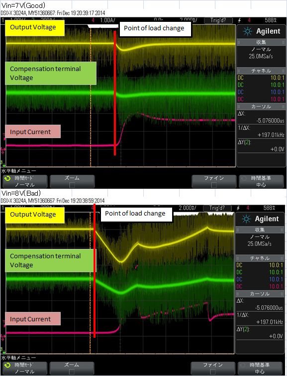
    Can we see waveforms on the COMP pin.FD
  • FD-san,

    Thank you for your help.

    I attach waveforms on the COMP pin.

    Please confirm them.

    Thanks and Regards,

    Kuramochi

  • The voltage on the COMP pin looks strange.  It should be going up during a load step from 0A to 400mA.

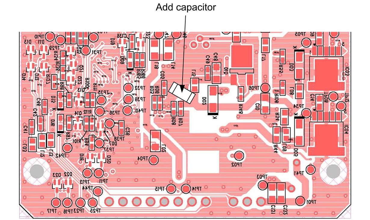
    You may have a ground loop on you PCB.  Can you show us you PCB layout.


  • FD-san,

    Thank you for your confirmation.
    I want to send PCB layout data by e-mail.
    Can you tell me your e-mail address?
    Or please send e-mail to me.
    There is my address on my profile page.

    Thanks and Regards,
    Kuramochi

  • FD-san,

    Thank you for reply.

    I have sent email to you.

    Thanks,

    Kuramochi

  • OK; We will look at it.
  • We have several suggestions and experiments:

    1. It looks like the biggest problem is connecting the top of the feedback resistor, R07 to the cathode of the diode.  This connection should be done at one of the output capacitors.  As an experiment, connect a 100uF, or so, capacitor from the cathode of the diode to the ground plane near the ground vias on the device.

    2. Another experiment is to remove the feedback divider and replace with resistors on top.  Connect the R07 to near C08 and ground R08 to near the ground on the device.

    3. Also, the grounding of the output capacitors is not good.  The grounds of all the caps should be very close to the ground on the device.  It is best to have all the output capacitors on the same side of the board.

    4. What is the purpose of L15 and the related components ??  I do not see them on the schematic.  Another experiment would be to remove them and see if that has any effect.

    5. Also it is best not to use thermal reliefs for power devices.

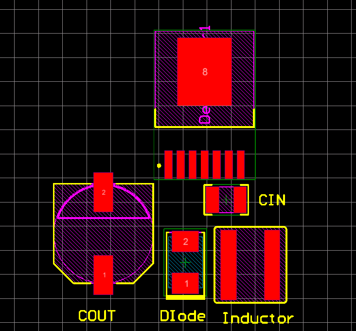
    6. I have attached some drawings for you to look at.


  • FD-san,

    Thank you for your comment and quick reply.
    I have informed my customer these information.

    If my customer has some question, I ask you again.

    Thanks and Regards,
    Kuramochi
  • We have looked at this design in our lab, and we see the same load transient that you are getting. The reason is that your load step is going from 0A to full load. This device has a "burst-mode" that is used when the load is small or 0A. In this condition the output of the error amplifier, COMP, can go very low with no load. When a heavy load is applied it takes a long time for the voltage on the COMP pin to rise up to command more inductor current. This long delay causes a large dip in output voltage. If a small constant load is applied to the output, such as 20mA; the problem is not seen. Another way to help this condition is to reduce the value of the compensation capacitor and inrease the value of the compensation resistor, by the same ratio. This will reduce the time constant of the compensation components and speed up the transient response. This must be done very carefully to make sure that the stability is not degraded. Testing over line/load and temperature would have to be done, as well as BODE plots. We also found that the 22uH and 200khz makes the condition worse. We would recomend 100kHz and 330uH. With the 22uH and 200khz, at least 100mA of constant load is required at Vin=12V for good performance. We also believe that the layout issues that we found previously are also contributing to this condition.
  • FD-san,


    Thank you for your comment.

    I have 3 questions.


    1. How does "burst-mode" work?
    (Is there anything to refer a document?)


    2. What is the condition to start "burst-mode"


    3. >We would recomend 100kHz and 330uH.
    Is the correct inductance 33uH?


    Thanks and Regards,
    Kuramochi

  •  

    1. and 2.  At very light or no load the output voltage will start to climb up, since the minimum duty cycle limit is being approached.  This causes the voltage on the COMP pin to fall low.  When the voltage on the COMP bin falls near about 0.3V, the switching action is turned-off.  This causes the output voltage to slowly fall.  As the output voltage falls, the voltage on the COMP pin will rise.  When the COMP pin voltage rises about 0.3V, switching action is resumed and the "burst" cycles repeats.  With a small constant load, the voltage on the COMP pin will never fall as low as 0.3V, and burst mode will not be entered.

    3. At 100kH and 330uH are correct; that is what WeBench gives.  This combination seems to help the condition you are seeing.

  • FD-san,
    Thank you for your reply.
    I understood.

    I have a question.

    Why does working of the voltage on the COMP pin change by the input voltage?

    Thanks and Regards,
    Kuramochi
  •  

    The voltage on the COMP pin is the output of the error amplifier and the input to the current mode comparator.  This voltage will change with the duty cycle and the inductor current.  The inductor current changes with load on the device.  So as the input voltage is changed the duty cycle will change and the voltage on the COMP pin must change. 

  • FD-san,

    Thank you for your support.
    My customer has solved the problems.

    Thanks and Regards,
    Kuramochi