This thread has been locked.

If you have a related question, please click the "Ask a related question" button in the top right corner. The newly created question will be automatically linked to this question.

TPS61220DCKT power ripple with new board design

We have a 6 layer board with the TPS61220DCKT to produce 5 volts for sensor power, backlight power, and other
features. Our first design had no issues with the 5 volt power. We made a couple of modifications to the board and now
have severe power ripple, and low power voltage (about 4.5 volts).

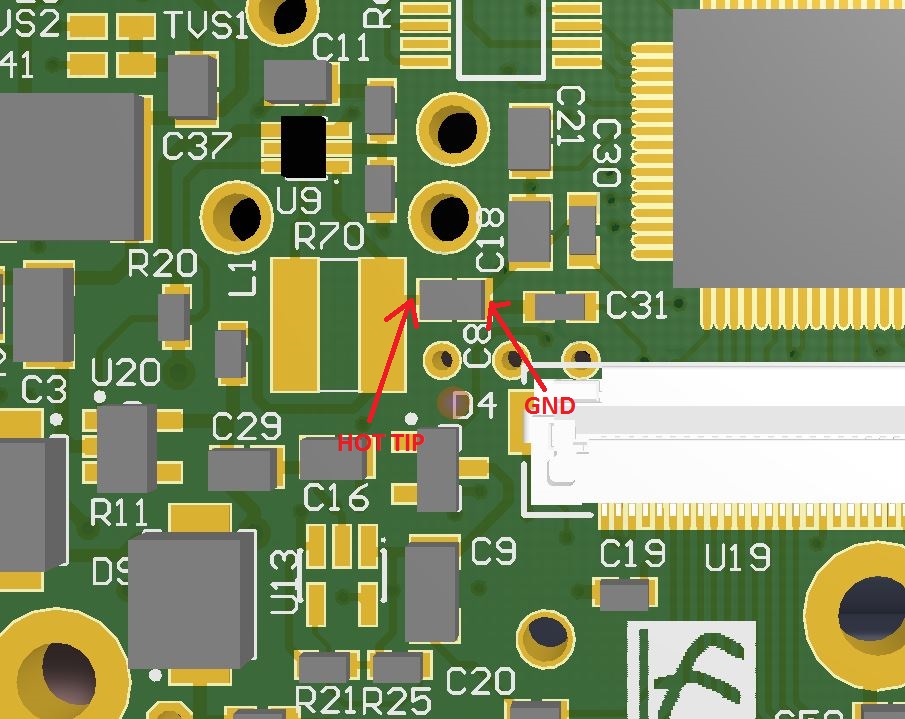
I've put together a 3 page PDF (mostly pictures) to explain the problem I'm seeing.

It can be viewed as this file:

TI Power Ripple.pdf

or at the link below:


  • Hi Kevin,
    There is several information I want to confirm with you:
    1) The modificaiton is just adding the on/off switch? Is there any change on PCB layout?
    2) You mentioned that change inductor helps to fix the problem, do they have the same saturation current? And what's total output load?
    3) It's weird that several minutes later, this problem can be fixed automatically. Could you please confirm is there any change several minutes later, for example, the output load or the input voltage?
    4) You mentioned using USB power made the case worse. So in your application, when using USB Power, the input and output are both 5V?

    BR
    Gene
  • Gene, thanks a bunch for looking at this. Here's some answers from my designer:

    1) The modificaiton is just adding the on/off switch? Is there any change on PCB layout?

    Yes, we also have moved and slightly re-arranged components, but noting critical.

    2) You mentioned that change inductor helps to fix the problem, do they have the same saturation current? And what's total output load?

    A new inductor has a smaller saturation current (0.48A) , but well into range of output current (0.1A).

    3) It's weird that several minutes later, this problem can be fixed automatically. Could you please confirm is there any change several minutes later, for example, the output load or the input voltage?

    The problem with old inductor (6.8uH) was very large inrush current, and very small duty factor. With 47uH we improved duty factor to about 50%, maybe we should reduce inductor to half value, 22-33uF?

    (from Kevin, the non-designer) It is likely "something" changed, like backlight went off and on, but something seemed to "fix it" if you waited long enough.


    4) You mentioned using USB power made the case worse. So in your application, when using USB Power, the input and output are both 5V?

    No output is 5.3V in both cases.
  • Hi Kevin,
    Here are some assumption and suggestion so that we can get more information and find the root cause.
    1) Is it possible for you to get the waveform of the inductor current? (both with output is OK and output is low with large ripple)
    2) Please make sure the output cap C11 is as close as to the IC or adding another cap close to the IC to see if it helps solve the problem.
    3) A smaller inductor is prefered to reduce the output voltage ripple.
    4) Remove (or short) the on/off switch (S2) to see if it is just same as your first design.

    BR
    Gene
  • Gene, I very much appreciate you taking the time for this.  My designer has answered these as follows:

    Here are some assumption and suggestion so that we can get more information and find the root cause.
    1) Is it possible for you to get the waveform of the inductor current? (both with output is OK and output is low with large ripple).

    No that’s impossible. No room for current probe, and also we don’t have expensive current sensing oscilloscope probe.


    2) Please make sure the output cap C11 is as close as to the IC or adding another cap close to the IC to see if it helps solve the problem.

    C11 is next to boost IC. Anyway I had experimenting with various arranged. No improvement.

    3) A smaller inductor is prefered to reduce the output voltage ripple.

    Smaller inductor makes high inrush current, which our circuit cannot handle.


    4) Remove (or short) the on/off switch (S2) to see if it is just same as your first design.

    Doesn’t help. I have tried that.

    Now, with a larger inductor of 47uH and with larger difference between Vin and Vout, the booster circuit works well.

    The problem occurs when voltage difference between Vin and Vout is small 0.3V.

    Do you have an idea how to solve this problem, perhaps with smaller inductor 22-33uH?


  • Hi Kevin,
    It makes sense when Vin is close to Vout, Vout ripple gets larger.
    Using a smaller inductor will increase the operation frequency and thus reduce the ripple, please use a 22uH to have a try, it should be better than 47uH inductor.
    Adding more cap at the position of C11 should have a benefit to reduce the output voltage ripple, but in your case there's no improvement. So would you please share your PCB layout since this part is sensitive to Cout cap position.

    BR
    Gene
  • We are going to try the 22 uH.  It will take about 5-10 days to send out some boards and get back.

    Here is board layout.  U9 is the TPS61220DCKT

    Notations in red are C11, R68, R70, C8 and L1 (top to bottom).

  • Hi Kevin,

    I checked the PCB layout and perhaps the following should have a better performance. Could you share the waveform of Vin when the ripple is large?

    BR

    Gene

  • Gene, my designer says:  

    I know that schematic, and I believe we are very close to it.

     I the attachment you can find the point for Vin measurement. Best way is to solder a small piece of wire to C8 and then attach scope probe.  NOTE:  I used a scope probe directly on C8.  Be sure to read more text at bottom of this reply.

    Here's a PDF of the VIN and VOUT with both USB power and then battery power .  These 4 pic were obtained with the new 47uH L1 component, which we are currently using as a fix..

    USB Micro Noise for TI Website.pdf

    I've learned more.  I tested about 8 boards with the original uH of 6.8 .  6 were pretty good for low ripple, 2 had the ripple.  This is a much lower percentage bad boards than in previous batches of boards I had tested.  In good and bad boards, you can see the VOUT goes to the lower voltage level 4.3 v with ripple shown in original document (boards with 6.8 uH), and then goes on to 4.95 volts within 1 sec or so for good boards.  

    The 2 bad boards stay at 4.3 w ripple.  They can eventually flip to 4.95 steady volts over time(20 sec to several minutes), or if I touch various components on the board.  I could not find 1 component that I could touch with my finger that would consistently fix it.  It is like some voltage level or spike, or capacitance level or something flips it into working correctly.  It is like something is in resonance, and once it gets fixed it says fixed, like an instability.

    I've also discovered that the USB power source has an effect also.  I tried 2 AC to USB power adapters and 3 laptops and 1 desktop.  One AC adapter definitely produced more of a problem with ripple.

  • Hi Kevin,

    The PCB layout is not so good.

    1) Long SW trace from L1 to SW pin of IC, introducing noise easily.

    2) Long GND trace between C8 GND and IC GND

    3) Long Vin trace from R11 to C8 and C8 to Vin pin of IC

    Both 2) and 3) make Vin worse and couples the noise to Vout.

    From your attached waveforms, we can find that pic1 and pic2 (USB powered) have the same frequency ripple (Vin and Vout coupled). However, pic3 and pic4 (battery powered) is quite good. And it is also mentioned that AC adapter makes things worse. So I guess noisy Vin and PCB layout bring in noise and couple it to Vout.

    Please make C8 closer to IC or enlarge C8 (for example 47uF or larger) or use RC (R11) to see if there is any improvement.

    BR

    Gene

  • Gene, thank you very much for your suggestions. This may not affect what you say, but I should say it. The VIN is very much influenced by the VOUT. On good boards when VOUT is clean, VIN is clean also. On bad boards, when VOUT has ripple, VIN has ripple also; then when VOUT goes clean, VIN is clean also.
  • Gene, I got 2 boards with 22 uH L1. Both seem to work very well. I did see the ripple on one board during one power up sequence (I believe w battery power only), but it went away by itself after about 5-10 sec. After that I never saw it again, either board, battery or USB power.

    What does that tell you?
  • Hi Kevin,

    It's better to have the waveforms if possible.

    From the description, I guess either it just trigger stability margin or some other function block power on/off in your system during that time.

    BTW, I still recommend change a better PCB layout and have a try. If it is really a stability problem, it's difficult to tell which trigger unstable first and which makes things worse, because Vin and Vout can interact each other. We need to exclude some factors and make our analysis easier and more focus.

    BR

    Gene

  • Gene, do you mean you would like to see pictures of the VIN and VOUT wave forms with the new 22uH?
  • Here's pics of voltage VIN and VOUT with 22 uH  L1.

    22 uH with battery power VOUT

    22 uH with battery power VIN

    22 uH with USB power VOUT

    22 uH with USB power VIN

  • Hi Kevin,
    Yes, the waveform changing from large ripple to small ripple if you can see it again.

    BR
    Gene