This thread has been locked.

If you have a related question, please click the "Ask a related question" button in the top right corner. The newly created question will be automatically linked to this question.

How to use LM5005 in inverting configuration

Other Parts Discussed in Thread: LM5005, LM5085, LM5008

Hi everyone

I need to design a negative power supply of -46V, 27mA from a positive voltage supply of 27.5V. I have posted here before and have been suggested to use LM5085 for inverting configuration, since I need a low current rated supply so I thought of using LM5005. I am having trouble deciding which configuration and formulas to follow for LM5005 since I could not find any note mentioning how an inverting configuration can be made from LM5005. I read slva317b as a reference for producing inverting  power supply from a Step-Down regulator but I am not sure if all those formulas apply to LM5005 as well as the pinouts of both the chips are slightly different.. Can we use LM5005 in inverting configuration? What formulas and requirements are necessary to use it in this configuration 

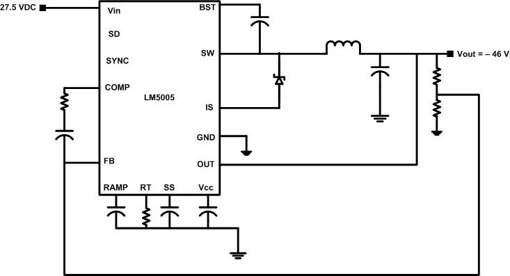
I extracted this schematic from LM5005 datasheet for using it in an inverting configuration. Do you think its going to work?


  • Hi,


    First off, the LM5005 can be used in an inverting Buck Boost. The simplest and crudest approach is to follow this Method.


    Make Vin = Modulus(Vout)+Vin

    Make Vout = Modulus (Vout)

    Make Iout = Iinave+Iout


    Where Iinave = Pout/Vin


    then run your calcs like a buck conveter.


    Compensation will be completely different but this can be tuned on the bench once up and running.


    I hope this helps?


  • Also please note that the schematic you have posted will not be representative of the LM5005 as a buck boost. The Gnd of the IC and all IC compoenents (Ref) will float to the negative output.
  • LM5008 should work. It is capable of handling the (46V+27V) with some margin. Integrated FET. COT is easy to use. No compensation. regards,
  • Hello David,

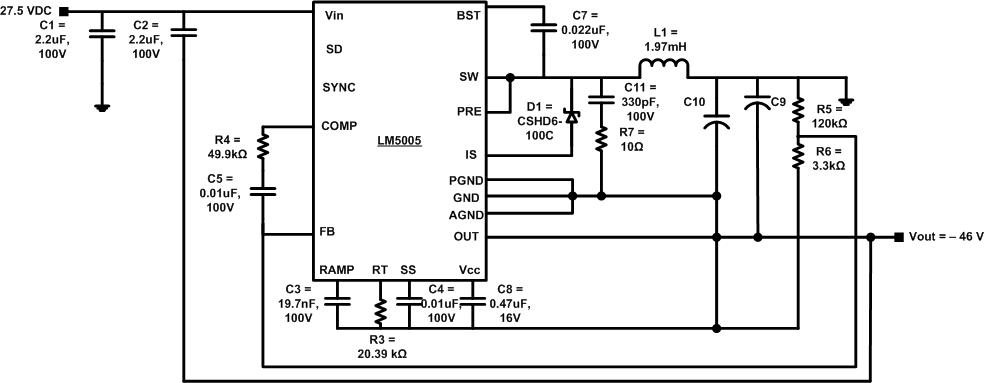
    How are you? Thanks for the reply. I followed the method you explained in your post earlier and then designed it like a normal buck as you suggested.I have edited my schematic, can you please review it and let me know if I did it all right?

    And yes I am having trouble deciding value for C9 and C10, what is the criteria for their selection? All the capacitors are ceramic as suggested in the datasheet.

    Thanks again! Here is the schematic

  • Hello Arhez,


    The output capacitor is chosen based on the output voltage ripple spec (as it supplies all the output current when the high-side FET is on). You can use a 1uF or 2.2uF 100V 1206 or 1210 ceramic cap (similar to what's used on the input). Also, you need to connect the OUT pin to the other side of the output cap (i.e. GND). As Vijay mentioned previously, the LM5008 COT converter is another option and might be an easier solution to implement.


    Regards,

    Tim 

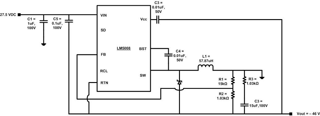
  • Thanks Timothy. I took your and Vijay's advice and used LM5008 as i can see the design is easier and more appropriate for this particular application, please review the schematic I am not sure about the inductor value I have selected I have used Vin = 27.5V, Current as 27mA, D = 0.625 and Fsw = 550kHz, I used the equation I used I earlier for LM5005 to calculate the inductor's value.

  • Does the Exposed Pad on the back of the device need to be connected to the negative output voltage, or is it not connected internally, and should be still connected to ground through vias for maximum heatsinking.
  • Please connect the DAP to the Gnd of the device which connects to the -Vout.

    kind regards.

    David.

  • David,

    could the part get damaged, if the exposed pad is connected to ground and not -VOut?

    Regards,

    Christian

  • Hello Christian,

    We strongly advise that the DAP is connected to the lowest potential that the device sees. If you connect the DAP to a higher potential other than the Gnd pin of the device, you could potentially set up cases for substrate injection (device failure). Please advise the designer to tie to the Ground pin.

    Hope this helps?

    David.
  • David,

    I have a question.  If the directions are to always tie the Pgnd to Agnd to the DAP, why isn't this done inside the package or even on the die itself?

    It seems to me this would be best for reducing parasitic inductance caused by external connection of these points.

  • Hi William,

    There are a few reasons, that I am not an expert on, but in general the reason is a mechanical construction challange to get the Dap conneted to Gnd without increasing the die size and package size.
  • Thank you David,

    we will correct that in the redesign.

    The problem is, that we have a prototype-board, with a buck converter from +24V to -19V, where the exposed pad is connected to ground (0V).

    There everything works fine for about half a minute, before output voltage drops down to about -5V, alltough there is no load and no output current.

    Because of the fact, that the same circuit worked well on another evaluation board, also with the exposed pad connected to ground, I'm not really sure if the connection of the exposed pad is really the problem or if there is another problem too.

    Best Regards,

    Christian

  • Hello Christian,

    There are also a number of other reason why this particular board is not working.  If the design works well on another board, it could be layout?  If the other board has the same layout it could be component differences?  In any case, we recommend the DAP to be connected to the lowest potential. 

    When you redesign the new board please make sure you follow the layout guidelines in the Datasheet.


    Hope this helps?


    David.

  • Hello David,

    we isolated the DAP from the -19V and it worked.

    I don't really know why it worked on my evaluation board where the exposed pad was connected to ground.

    I assume that it is a combination of the DAP connected to ground and layout, why it works at one board and fails at the other?!

    Maybe you should mention that DAP should be connected to the lowest potential in future datasheets.

    Thank you very much for your support.

    Christian