This thread has been locked.

If you have a related question, please click the "Ask a related question" button in the top right corner. The newly created question will be automatically linked to this question.

TPS62110 Vout fluctuates - will not maintain regulation

Other Parts Discussed in Thread: TPS62110

See the attached schematic and BOM. The output is set to 12V. The input is typically 14.4V (battery pack) but will gradually decrease. The no load output is 12V. Load testing with resistors shows large fluctuations in output voltage from 12V down to 10.5V as the input decreases to 12V. The load resistor is 30 ohms. I have built several boards and none perform properly.

TPS62110_12V.pdf

TPS62110_12V_Bom.txt
Qty Device      Value        Manufacturer Part Number         Parts 
1   CAP-0402    1uF          TDK          C1005JB1V105M050BC  C3    
1   CAP-0402    22pF         Murata       GRM1555C1H220JA01D  C4    
1   CAP-1206    33uF         TDK          C3216X5R1E336M160AC C1    
1   CAP-1210    10uF         Taiyo Yuden  UMK325BJ106MM-T     C2    
1   IND-SRU5018 6.8uH        Bourns       SRU5018-6R8Y        L1    
1   RES-0402    71.5k        Samsung      RC1005F7152CS       R1    
1   RES-0402    680k         Samsung      RC1005F684CS        R2    
1   TPS62110RSA TPS62110RSA  TI           TPS62110RSAR        U2    

  • Hi Will,

    If the input decreases to 12 V the Device should go in the 100% mode to achieve the 12V on the output.
    Which type of battery do you use?

    Could you post the layout?

    Thanks & Regards,
    Michael
  • Hi Mike,


    I understand the device has a 100% duty cycle capability. That's a good feature. It has not yet been used with a battery. All testing has been done using a bench supply. I have built several boards. The problem is the device will not hold regulation even under light load. I have attached the layout. Can I ship a unit to you?

    Thanks,

    WillTPS62110_12V_Layout.pdf

  • Hi Will,

    thanks for the layout. You will have to change a few things to get a proper working power supply.
    Please follow the layout recommendations in the DS on page 18. ( www.ti.com/.../tps62110.pdf )

    1. Place the input cap between Vin and PGND as close as possible to the device like on the EVM . www.ti.com/.../slvu135.pdf
    (In your current layout the current return path of the input cap goes over the AGND. This could lead to massive noise on the AGND. )

    2. Create a start point where you connect the AGND to PGND/GND like on the EVM.

    I would recommend to order the TPS62110 EVM to evaluate the Device. It has a good known layout.

    Thanks & Regards,
    Michael
  • Hi Mike,

    I do not understand what you mean by "Create a start point where you connect the AGND to PGND/GND like on the EVM"

    1)  It may not have been apparent from the layout file I sent you, but this is a 2-sided board and the bottom is a copper pour connected to ground. All grounds are connected. From what I can tell the EVM has the bottom layer connected to PGND only and PGND is isolated from AGND except where AGND is connected to the thermal pad. Is this the critical difference between the two layouts?

    2) From what I can tell the EVM has GND connected directly to PGND. Is that correct?

    3) Are there any other pin compatible devices that can provide 12V output at about 1A?


    Thanks,

    Will

  • I think Michael is out of the office today. He may not be able to answer quickly. Please stand by.
  • Hi Will,

    sorry this was a typo. I mean a 'star' point.

    1) Yes this is exactly the difference. PGND to AGND connection on a single 'star'point.

    2) Yes correct.

    Again, the input capacitor is the most important component for reliable operation of any step-down converter.
    Please place the input capacitor between Vin and PGND as close as possible to the device like on the EVM.

    3) I don't know a pin compatible device.

    Thanks & Regards,
    Michael
  • Hi Mike,

    I changed the layout according to your recommendations and followed the EVM layout as closely as possible. The new board has exactly the same problem as previous versions. There is absolutely no change in performance. The converter will not maintain regulated output. I have attached the new layout.


    Will

    TPS62110_12V_Layout-2.pdf

  • Can we see the regulation graphs? Even at 100% duty cycle there will be some loss in the high side FET
  • Hi John,


    I would like to send you the completed PCB. What address should I send it to and to who's attention?


    Thanks,

    Will

  • I don't directly support TPS62110. It belongs to a different business group, but since I am the technical owner of this forum I tend to post in threads not directly related to parts i actually support. If you could just post Vout vs Vin ( if I follow this correctly, that is your issue, correct?), maybe we can resolve it on line. Otherwise, Michael will be your direct support.
  • Hi John,


    Will Mike be able to help when he is available? A graph is not necessary. For example, at Vin = 14.4V the output is 10.5V with a 30 ohm load. Can someone verify the layout I posted? I have spent too much time on this device already but I would like to know why I can't make it work. I'm at a point where the best thing for me to do is to send Mike a unit so he can see what I'm talking about. There is no sense kicking this around like a football.


    Thanks,

    Will

  • As you are probably aware it is a holiday weekend. Let me see what we can come up with next week.
  • Hi John,

    thanks for following the layout guidelines.
    To help you we need more information's.
    Could you please post a scope plot of the load step? With Vin, Vout, Inductor current.

    Additionally you could put the unit on a TI EVM and see if the issue is still there.

    Thanks,
    Michael
  • Hi Mike,

    I can't provide scope plots. I can send you a device. I have customers who are looking for a solution. Maybe this device is not suitable. I have spent too much time with this device. I have used TI converters in the past with good success. I simply cannot kick this back and forth on this forum. It is much too time consuming. EVMs are nice for evaluation but I need to provide a product.

    If you are unable or unwilling to accept the device I have can you pass this issue on to someone else.


    Thanks,

    Will

  • Hi Will,

    I understand that your customer need a solution.  But i need more information's to help you.

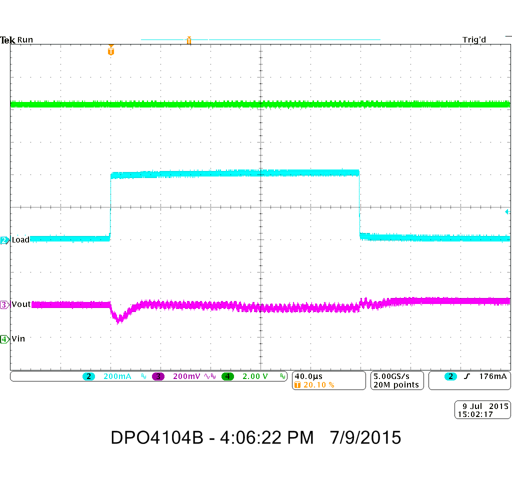
    I performed a measurement on my bench with your conditions. 14.4Vin, 12Vout, 400mA load step. The device operates as expected.

    Could you please also provide such a waveform?

    In addition, can you please try to increase your output capacitance and check if there is any difference?. e.g. 68uF

    Shipping a device makes no sense. So far it looks like its not related to the device. 

    Thanks & Regards,

    Michael 

  • Hi Mike,

    Have you looked at the new layout I posted? See the attached graph. The load is a 30 ohm resistor. Adding more output capacitance reduced the ripple but nothing more than that. I did not mean to send a device as in the converter chip itself but rather the completed PCB as I indicated on July 3.

    Thanks,

    Will

    load_in.pdf

  • Hi Will,

    Yes, they layout is good.  It is quite the same as the EVM. No issues from that side.

    Thanks for the scope plot. Did you connect the scope probes directly at J1 and J2?

    Did you try adding more capacitance? I ask because the output capacitor you used have a really strong derating due to DC bias.

    With 12V there are only ~4uF left. In addition you have a +-20% tolerance.

    With such a low output capacitance the converter may cannot operate in a proper way. 

    Thanks & Regards,

    Michael

  • Hi Mike,

    As you can see the PCB is small. I have flying leads soldered to J1 and J2. This is where I make measurements. As I indicated in my last post I tried adding more output capacitance. Adding more output capacitance reduced the ripple but nothing more than that. What output capacitance did you use on your EVM? I followed the guidelines in the datasheet when selecting the output capacitance value. I would use a larger capacitor for future builds if it worked.

    Why are you unwilling to look at the completed PCB? How much more can we do on this forum?


    Will

  • Hi Will,
    thanks for your answers.

    In general we are encouraged to support and solve customer issues trough the E2E. This works in most cases.
    Please send me an email and i will provide you a address where to ship your board: m-helmlinger@ti.com

    Regards,
    Michael
  • Hi Mike,

    I found that by removing the feedback capacitor (Cff or C4 on my schematic) the output voltage would not drop when the load was applied. So this was a significant improvement. However, it seems that having no feedback capacitor causes inaccurate output voltage. What should be 12V +/- 1% is actually more like 12V +/- 10%.

    The initial value of Cff was 22pF. I also tried 4.7pF. Using either of these results in the original problem.

    What value of feedback capacitor would you suggest?

    Thanks,

    Will

  • Hi Will,

    I used the standard TI EVM with 10pF feedforward capacitor and it works as expected. No voltage drop.

    You could test your circuit with the TI EVM and see if it works. Then you could replace your passive components with the components on the EVM and see if this helps.
    The other option is to send me your pcb.

    It still would be good to get a scope plot.

    Thanks & Regards,
    Michael