This thread has been locked.

If you have a related question, please click the "Ask a related question" button in the top right corner. The newly created question will be automatically linked to this question.

LM5119 - design help

Other Parts Discussed in Thread: LM5119

Hello,

 I'm designing new PCB with LM5119 and have one question. Can I put 2 FET's in parallel and connect to HOx & LOx or I need to put FET driver between LM5119 and each FET? I want to put 2 FETs for hight & 2 FETs for low side for each rail to reduce heating of FET & spread heat over PCB.

Thanks and kind regards,

 Mladen

  • It is ok to drive two FETs with each driver so long as the total gate drive capability is not exceeded. See this reference design as an example:
    www.ti.com/.../tidre12
  • Hello,

     I need little help with LM5119. I design PCB for 12V/10A & 5V/5A outputs. When I power up PSU, won't star up. In design, I use PMP9260 & SNVA444B schematics. Some of value from design, tss=10ms, fsw=99,9kHz (I also try with 216kHz), tRES=58.75ms, K factor for CH1=2.609, K factor for CH2=2.44
    I measure voltages on some pins:

     - Vin=36.1V

     - Vcc1= 0.417V

     - Vcc2= 0.68V

     - UVLO=1.875V

     - EN2= 3.97V

     - RT= 1.96V

     - VccDIS= 0.152V

    On VccX should be around 7.6V by the datasheet. Can you please give me advice what can I check or try to start up PSU?

    Thanks & best regards,

     Mladen

  • Hi
    Please remove the external VCCX circuit, VCCDIS circuit and check each nodes one by one.
    -UVLO should be higher than 1.2V
    -VCC should be in regulation
    -SS should be high state
    -COMP should be high state
    -FB should be around 0.8V.
    Regards,
    EL
  • Hi,

    Sorry for late replay, but we have holidays. I solder new PSU and it's working, but no I have another "problem". Low side FET's for 12V it's little worm without any load at output (diode emulation pin is floating). And I have one question, PSU will be loaded with around 6.5-8A on 12V/10A chanel & around 2-3A on 5V/5A chanel. Can you please advice me if is better to use diode emulation on it's better to disable emulation for the nominal load?

    Thanks and best regards,

    Mladen

  • Hi Mladen

    Diode emulation mode is recommended in general.

    Regards,

    EL

  • Hi Eric,

     I need again help. PS is working ok if current consumption is less than 1A on any output. If current consumption is more than 1A voltages on outputs drop on half of nominal value (12V output drop on 5.6-5.8V, 5V out drop on 2.3-2.6V). 12V output is designed for 10A and 5V output is designed for 5A.

    Can you please suggest me what to check or try. I try to change switching freq form 99.9kHz to 211kHz, but result was same.

    Thanks and best regards,

     Mladen

  • Hi Mladen
    Please enable hiccup mode by adding a capacitor at RES pin
    And then check if RES is moving up and down when you see the issue
    If RES pin voltage is moving up and down, your PS is in current limit.
    Regards,
    EL
  • Hi Eric,

     Seems like PS is in current limit. Voltage on RES pin is look like charging capacitor graph. I'll look into datasheet how to solve this problem.

    Thanks and best regards,

     Mladen

  • Hi Eric,
    Sorry for bothering you again, but I still need help. PS was in current limit, so I change Rs and make new calculation for Rramp and change fsw to 211kHz. But PS was still in current limit. I remove capacitor from RES pin and connect RES pin to VCC1.
    After that I have on 12V (CH1) 2.3A (I don't have "bigger" load atm to test), but 5V (CH2) output after current exceeds 0.1A voltage drop to around 2.3V and return back to 5V. I noticed that CH2 have a lot noise on output.

    Can you please help with this problem.

    Thanks and best regards,
    Mladen
  • Hi Mladen

    - Please check your power supply has enough capability to handle the maximum power

    - Please enable only one channel and test one by one

    - Increase Css dramatically (10 x Css ~ 100 x Css ) 

    - Consider a RC filter at CS-CSG

    Regards,

    EL

  • Hi Eric,

    - Please check your power supply has enough capability to handle the maximum power

    - I have power source that have 35V/6.25A output, that should be enough power.

    - Please enable only one channel and test one by one

    - I'm testing one by one channel. Looks like CH1 now working OK ( I have load on my table that can handle 2.5A on 12V and that's working now). But when I strat testing CH2, I can get only 150mA. At that current voltage drops below 3V.

    - Increase Css dramatically (10 x Css ~ 100 x Css ) 

    - I add 1uF and 2.2uF but still can't get more than 150mA on CH2 and there is still noise on CH2 output. By default was 100nF.

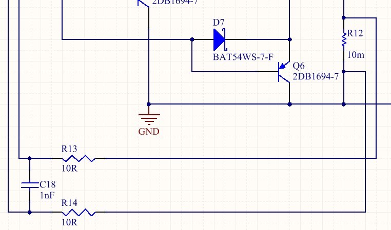
    - Consider a RC filter at CS-CSG

    - I have RC filter, this is screenshot of schematic.

  • Hi Mladen

    Would you please let me know each pin's status when you test only CH2? Especially, VCCDIS, VCC, COMP, SS, RES

    Regards,
    EL
  • Hi Eric,
     Here is status of the pins:
    - VCC1=7.46V
    - CGS1=1.5mV
    - CS1=2.5mV
    - RAMP1= 3.5mV
    - SS1=3.1V
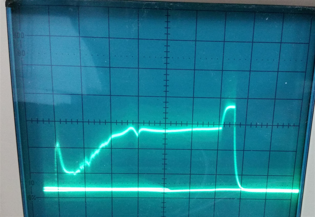
    - VCCDIS=100mV (min) - 800mV (max)

    (sorry for picture, but atm I have only old scope, new one is on service)

    -FB1=0.8V

    -COMP1=1.26V

    -EN2=4.85V

    -RT=1.26V

    -RES=7.5V (connected to VCC1, if I put capacitor then I can't get more then 1A on CH1 )

    -COMP2=0V

    -FB2=0.4V

    -DEMB=95mV

    -SS2=2.5V

    -RAMP2=11.5mV

    -CS2=4.9mV

    -CSG2=4.9mV

    -LO2=6.6V

    -VCC2=7.1V

    -SW2=6V

    -HO2=6V

    -HB2=6V (with 6V offset)

    -UVLO=1.887V

    -VIN=35.3V

    -HB1=14.4V

    -HO1=12.65V

    -SW1=12.15V

    Regards,

     Mladen

  • Hi Mladen

    Which node waveform did you capture? 

    How can SW1 be 12V when only EN2 is working?

    Is LO1 DC ? no pulse????  

    COMP2 should be high state when FB2 is lower than 0.8V. Please check compensation component connections.

    Regards,

    EL  

  • Hi Eric,

     Waveform from previous post is on VCCDIS.

    SW1 and LO1 are pulses. LO1 is 0.2ms in high state.

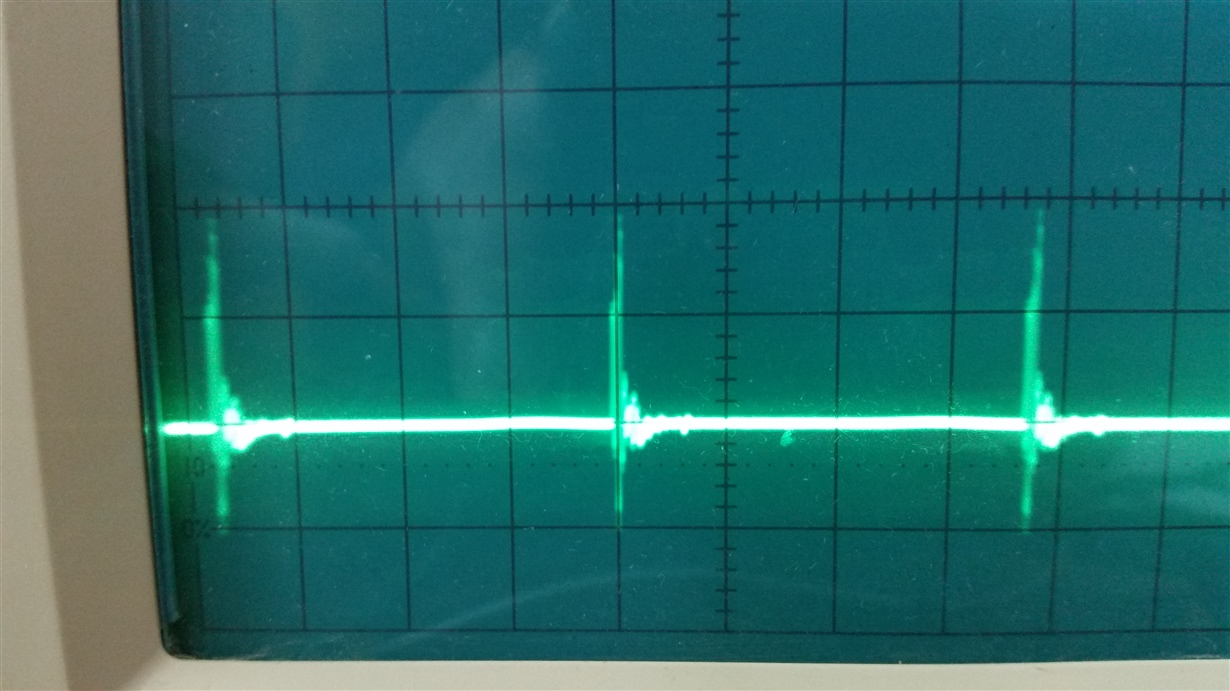
    Here is waveform of COMP2 pin (0.5V/div, 0.5us/div)

    FB2 is DC and it's 0.4V.

    I'll change low side FETs, I tested all FETs and look like one or both CH2 FETs are shorted.

    Regards,

     Mladen

  • Hi Eric,
    I solder new PS, but it's same problem. CH1 (12V) working OK but on CH2 (5V) I can't get more than 0.23A (from time to time I get 0.25A for less than second) and voltage drop on 2.35V (load is 10R resistor).
    I disabled hiccup mode.
    Can you please give me advice what to do/check?

    Thanks and best regards,
    Mladen
  • Hi Mladen

    If there is no abnormal difference between two channels on your schematic, I think you should check your board if any mistake or error.

    It seems like CH2 is current limited. Usually, by reducing Rs or by adding a RC filter, the issue is resolved.

    Regards,

    EL

  • Hi Eric,
    Only difference between channels are, RS CH1=10m, CH2=5mR; RC are same, inductors are 33uH (CH1), 10uH (CH2); compensation network are different CH1 Rcomp1=23.7k, Ccomp1=6.8nF, Chf=100pF, CH1 Rcomp2=16.5k, Ccomp2=10nF, Chf=220pF (values that I got from web designer). Rest of components are same.

    Regards,
    Mladen