This thread has been locked.

If you have a related question, please click the "Ask a related question" button in the top right corner. The newly created question will be automatically linked to this question.

TPS40140 : MOSFET going bad

Other Parts Discussed in Thread: TPS40422, TPS40140

We are using TPS40140 for converting 12V to 1V8 (1.8V).

It has been observed that the MOSFET used (IRFH7914) is burning after board is powered on and is working for few days and as a result a 12V to GND short is observed.

There is gate series resistor (10 ohms) for each MOSFET.

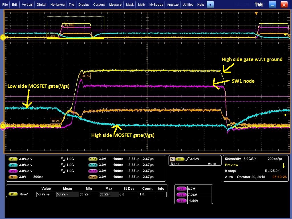
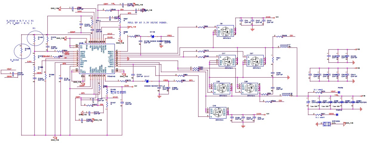
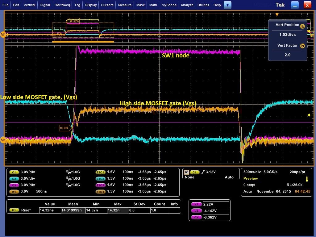
To debug this issue , we have probed few nodes in the circuit(High side MOSFET gate to source,Low side MOSFET gate to source,SW1 node,High side MOSFET gate w.r.t ground).The schematics and waveforms are attached.

1)We are able to see an overlap of High side MOSFET gate to source and Low side MOSFET gate to source waveforms when Low side is switched OFF and High side is switched ON.Whether this will cause cross conduction and whether this is the reason for MOSFET going bad?

2)whether replacing gate resistor by 0 ohm will result in faster turn OFF of low side and may solve above issue?But this will result in faster turn on also.please suggest how to solve this issue?

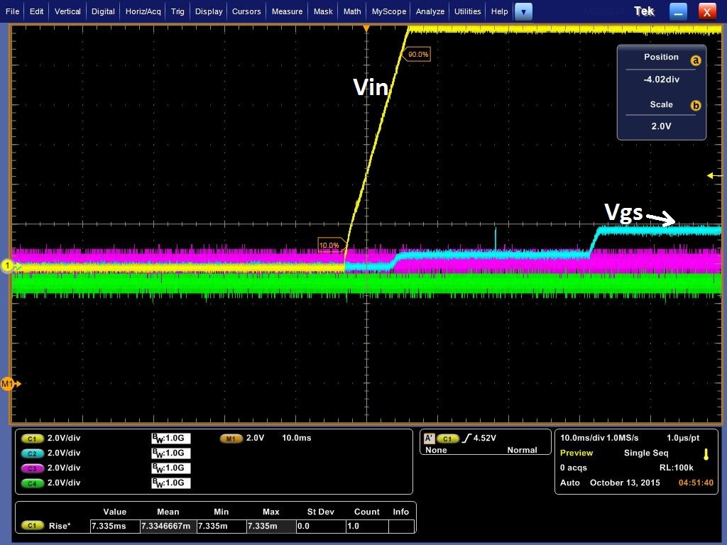
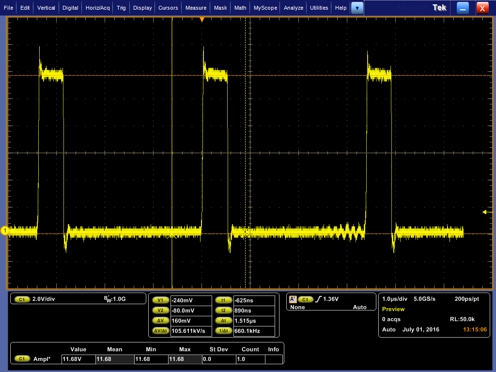
3)We also observed some gate voltage(around 1V) during start up.The waveform for the same is attached.Whether this also can cause MOSFET to go bad?Whether any pull down resistor(between gate and source) for each MOSFET is required to solve this issue?


  • Schematics and Wave forms are attached here   .

  • Hello,

    It is highly possible that the FET failure is caused by the overlap bettween HS-VGS (high side gate to source) and LS-VGS (low side gate to source).
    There should be a dead time between HS-VGS and LS-VGS to avoid short-through.

    Please change low side gate resistor to 0ohm and reduce high side gate resistor to several ohms (2 to 5 ohm)

    Thanks
    Qian
  • Hi,

    Can you please explain why we are providing different gate resistors for High side and Low side MOSFET? What is the difference in the effect?

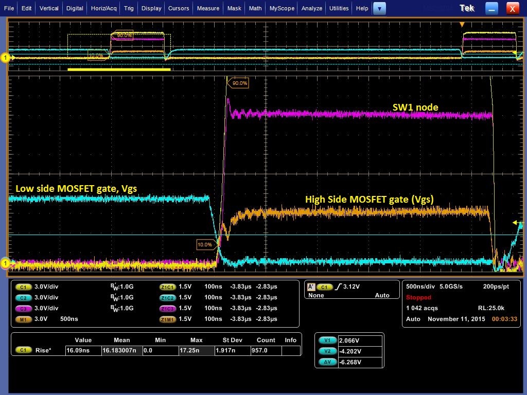
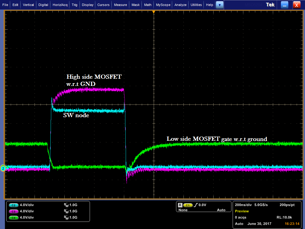
    The waveform for High side MOSFET with gate resistor 2.21 ohm and Low side MOSFET with 0 ohm resistor is as shown below:

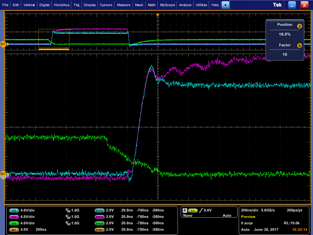
    The waveform with all the gate resistors to be zero ohm is as shown below:

    Please see this and suggest further measures to be taken.

    Regards,

    Rasif

  • Hi Rasif,

    The HS gate resistor is to slow down HS FET turn-on, hence to reduce the voltage spike on switch node. You also can use boot resistor to slow down HS FET turn-on.

    The LS FET needs to be turn on and off quicly, therefore the LS gate resistor can be 0 ohm.

    I see there still some overlap between LS-VGS and HS-VGS when LS FET is off and HS FET is on.

    Can you check if the failure goes away after change gate resistors?

    Thansk

    Qian

  • Hi Qian,

    1. Since we have seen the waveform with HS gate resistor = 2.21 ohms and LS gate resistor = 0 ohms. We have also seen the waveform with both HS and LS gate resistor = 0 ohms, in the previous reply of mine.

    As we still can see the overlap, what is the next change in gate resistor, that I should go for?

    2. From the schematics, you can see that boot resistor is 4.7 ohms. How should I change this to better the scenario and complete avoid the overlap between LS-Vgs and HS-Vgs? What is the calculation for this? 

    Thanks and Regards,

    Rasif

  • Hi Qian,

    Also, please note that there is a initial gate voltage of 0.5V - 1V during the startup. Is this expected or will this be another cause for the issue?

    Do we have to provide a pull-down resistor to pull this voltage to 0V ?

    Regards,
    Rasif
  • Hi Rasif,

    The overlap only happens when HS FET is on and LS FET is off.

    Please increase HS gate resistor (Rg) value to slow down the turn-on of HS FET, hence to reduce overlap between HS-VGS and LS-VGS. Meanwhile, add a schottky dioe Dg in parallel with Rg as below figure shows to keep HS FET being turned off quickly.

  • The figure how shottky diode Dg is placed can be found on latest TPS40422 datasheet page 19, figure 13
  • Please add a 10k resisstor between FET gate and source to see if the initial gate voltage is eliminated.
  • Hi Qian,

    What are the parameters that I should consider for selecting the Schottky diode? The datasheet of TPS40422 mentions only the orientation of the diode to be placed.

    And, is there any calculation for selecting the optimum value of the gate resistor?

    Thanks and Regards,

    Rasif

  • HI Rasif,

    The forward coduction voltage of schottky diode must be lower than the MOSFET turn-on threshold with margin. Therefore the MOSFET keeps off when the gate drive signal is low.

    As long as dead time is sufficient, the gate resistor value should be small to reduce the switching loss.

    The value of gate resisor needs to be determined by test result.

    Thanks

    Qian

  • Hi Qian,

    We are placing the passive circuit consisting of the Gate resistor, bypass Schottky diode and the Pull down resistor for the HS MOSFET.

    Are we supposed to place the same circuit for the Low Side MOSFET also?

    Thanks and Regards,

    Rasif

  • Hi Rasif,

    Though the test waveform shows only the turn-on of HS FET needs to be delayed to increase the deadtime, I suggest to place the same circuit for the low side MOSFET as well in case the turn-on of LS FET needs to be delayed in the future. The gate resistor of LS FET can be 0ohm if the delay is not needed.

    Thanks

    Qian

  • Hi Qian,

    We are using SB180 as the diode considering the only parameter as Forward conduction voltage of diode to be less than that of Vgs (threshold).

    The datasheet has been attached herewith.

    Please tell if any other parameters need to be considered for the diode selection such as the current capacity, power dissipation etc.

    Regards,

    Rasifds30116.pdf

  • Hi Rasif,

    I think you can consider SMT package for the diode, because SMT package has smaller parasitic inductance.

    Besieds the forward conduction voltage, select a diode with high forward current (>1A) capability, so the FET can be turned off quickly to reduce switching loss.

    Btw, do you see a thermal problem on FET? If yes, probably a seperate strong FET driver is needed.

    Can you contact me by email: Q-CHEN AT TI.COM?

    It is more convenient to discuss by email.

    Thanks

    Qian

  • Hi Qian,

    We tried changing the resistor values on HS FET to 2.2 ohms and LS FET to 0 ohms. The Voltage was fine initially and the system worked for 3-4 days. Later the voltage has dropped down to 0.64 V. We have checked if the MOSFETs went bad, but there is no short as such from source to Drain.

    Is there any chance that this might have affected the TPS40140 IC ?
    We have tried this on two systems and both the results are same. (Anyway we did not use any diode while testing, will it affect?).
  • Hi Giridhar,

    Can you replace the controller to see if the problem is caused by TPS40140?

    If the problem goes away with a new controller, can you check below items?

    -Check if there is overlap between HS gate signal and LS gate signal

    -Check if voltage spike on BOOT pin and SW pin is beyond the ABS spec.

    Thanks

    Qian

  • Hi Qian,

    We have replaced the controller and there is no difference in the output voltage. It is still at 0.7 V. We have also checked for any Mosfet damage or any component lost in the circuitry. But the Mosfets and components are fine. The issue may not be with the controller going bad, we are working on it. It would be helpful if you can look into this and suggest some debugging.

    Thanks

    Giridhar

  • Hi Diridhar,

    Can you check the FB and COMP voltage?

    Also, please provde the SW and VOUT waveforms.

    Thanks

    Qian

  • Hi Qian, 

    The measured voltage values for pin FB is 200mV and pin Comp is 800mV in the system  with 1V8 issue. 

    Whereas in working sytsem, voltage values for pin FB is 700mV and pin Comp is 2.2V 

    Also the waveform for SW pin is attached and Vout voltage is 0.65V 

  • Hi,

    If FB is 0.2V, COMP should be high to make Vout regulated, but you said COMP is only 0.8V.

    Can you provide the latest schematic in pdf file?

    Thanks

    Qian

  • Hi Qian,

    The schematic for 1V8 is attached in here. The gate resistor values for HS Mosfets is 2.2 ohms and LS Mosfets is 0 ohms.

    /cfs-file/__key/communityserver-discussions-components-files/196/1V8.pdf


    Regards

    Giridhar

  • Hi,

    The schematic looks fine. Can you provide the waveform of below pin?

    VOUT, SW, TRK1, COMP

    Thanks

    Qian

  • Hi,

    As per the observations done on various pins of TPS40140 of 1V8 circuit, the following are the values.

    FB pin :  200 mV  

    Comp pin : 600 mV

    Ilim pin : 2.9 V

    TRKx pin : 600 mV

    The following values should be square waves with some duty cycle. But these are also constant at given values. 

    Boot pin : 500 mV (constant  value - no switching)

    Sw pin : 800 mV   (constant  value - no switching)

    HDRV pin : 800 mV  (constant  value - no switching)

    Earlier the Sw pin was switching in this system, and the waveform of the same was attached in earlier reply. Now it has become constant at 800 mV.

    This is some observation we made which may be relevant. The source and drain resistance value of High Side Mosfet in this system has come down to 1.56 Kohms whereas in other working systems, this value is 3.56 kohms.

    Thanks

    Giridhar

  • Hi Qian,

    We had revised the design as per your suggestion and these are the waveforms we are getting:

    1. We have used high side MOSFET gate resistor as 22.1ohms and low side MOSFET gate resistor as 10ohms, with a parallel diode respectively. Now the overlap has reduced and is very little resulting in very less cross conduction compared to previous case. Though there's switching loss due to 22.1ohm High side gate resistance, but the MOSFET can be saved.

    2. The schematics is as shown below:

    0753.1V8.pdf

    You can see we have also connected a 10K between gate and source for both High side and Low side MOSFET.

    3. The issue now is we are still observing that Q9 and Q10 (high side MOSFETS) are going bad. 

    4. Can you please see the schematics and point out issues, if any. Also can a faster turn off of the Low side MOSFET cause a high dI/dT resulting in reverse recovery issues?

    5. Is the 10K resistor between gate and source fine? Is there an issue with that?

    Can you please reply on this urgently. The project is held up due to the same.

    Regards,

    Rasif

  • Zoomed in waveforms. 

  • Hi Rasif,

    What test condition did you see the high side FETs are damaged?

    What's the failure result, drain to source short, drain to source open or other?

    Do you have a thermal camera to check the FET temperatuer?

    The 10kohm resistor between gate and source should not be related to the FET failure.

    The faster turn off of low side FET is not related to the reverse recovery of bode diode.

    Thanks

    Qian

  • Hi,

    We have powered it up under no load and very less load compared to the design. We have observed drain to source short.

    Also, earlier we the MOSFETs used to go bad after a period of operation, more than 6months. After the recent revision of schematics, the MOSFETS are going bad on power up itself.

    Yes, we have a thermal camera. We'll check on this and get you results. 

    Can you please explain if there's a DEAD TIME inherent to the IC working? We saw a Anti-cross conduction block in the datasheet, can you please explain what is about?  

    Regards,

    Rasif

  • Hi Rasif,

    There is adaptive dead time circuit inside IC.
    Your waveform shows the LDRV falling edge is slow. Can you change LDRV gate resistor to 0ohm and test again?

    Thanks
    Qian
  • Hi Qian,

    We had earlier attached the waveform with LDRV gate resistor as 0ohm and posted it in the thread. Can you please check it?

    Also, In the schematics, you can see a Schottky diode parallel to the LDRV gate resistor. Isn't it as good as placing a zero ohm resistor, for turn off?

    And, if there's an adaptive dead time circuit in the IC, why are we seeing an overlap between both the waveforms?

    Regards,

    Rasif