This thread has been locked.

If you have a related question, please click the "Ask a related question" button in the top right corner. The newly created question will be automatically linked to this question.

Spikes on LM3481 Vout

Other Parts Discussed in Thread: LM3481

I am developing a dc/dc sepic converter using the lm3481.

these are the parameters:

Vin: 9V - 32V;

Vout: 12V

Iout (max) = 3A

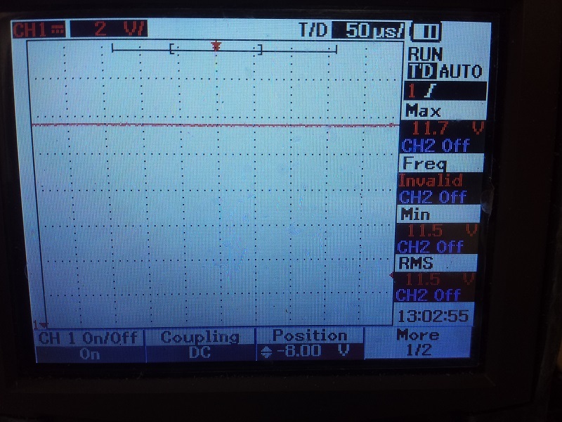
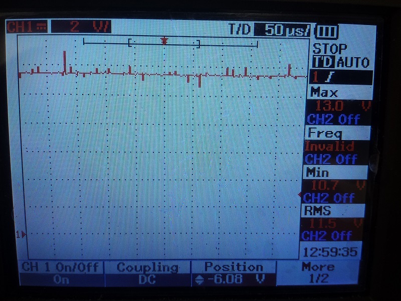
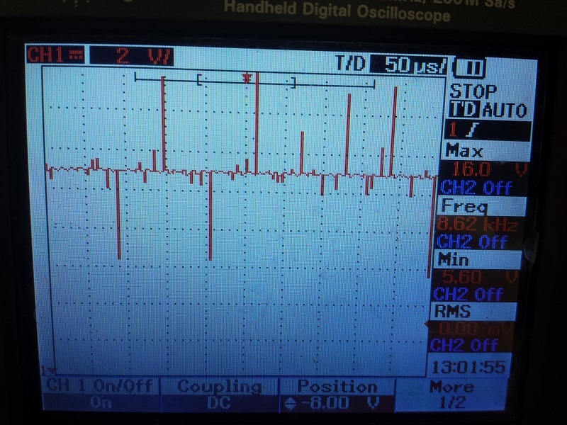
When my device is On with no load the regulation looks OK. But when I increase the load it starts to show some spikes on Vout.

It seems to be the same problem of another post  (LM3481 Sepic Circuit, Spikes on Vout), still not solved.

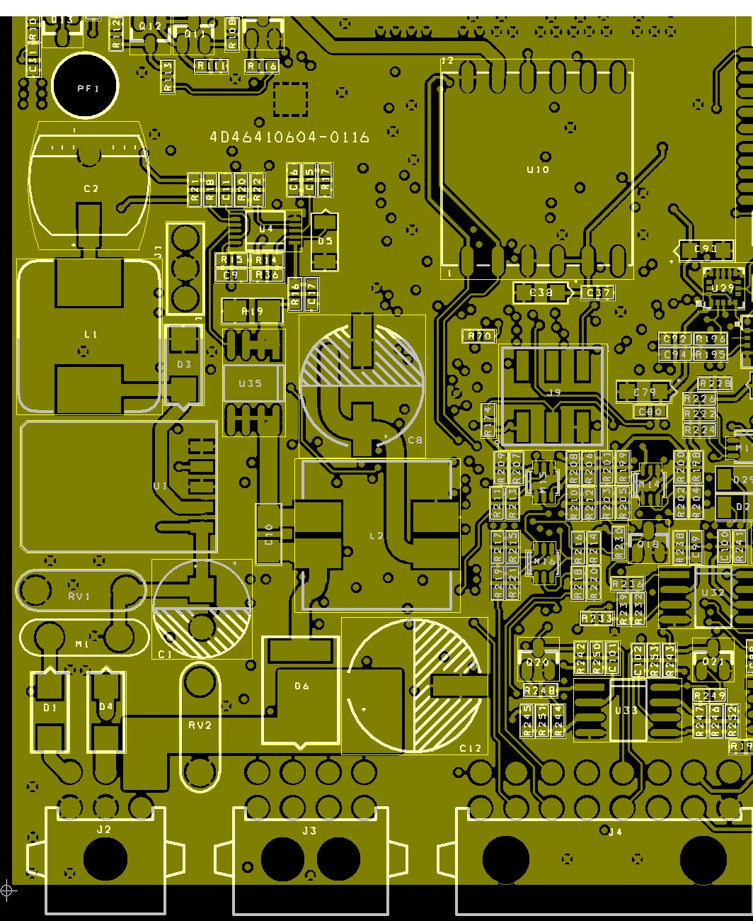
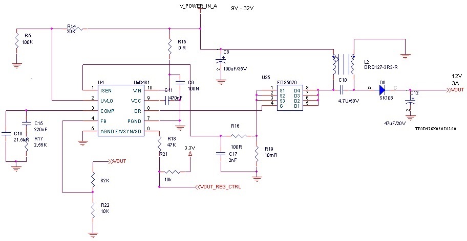
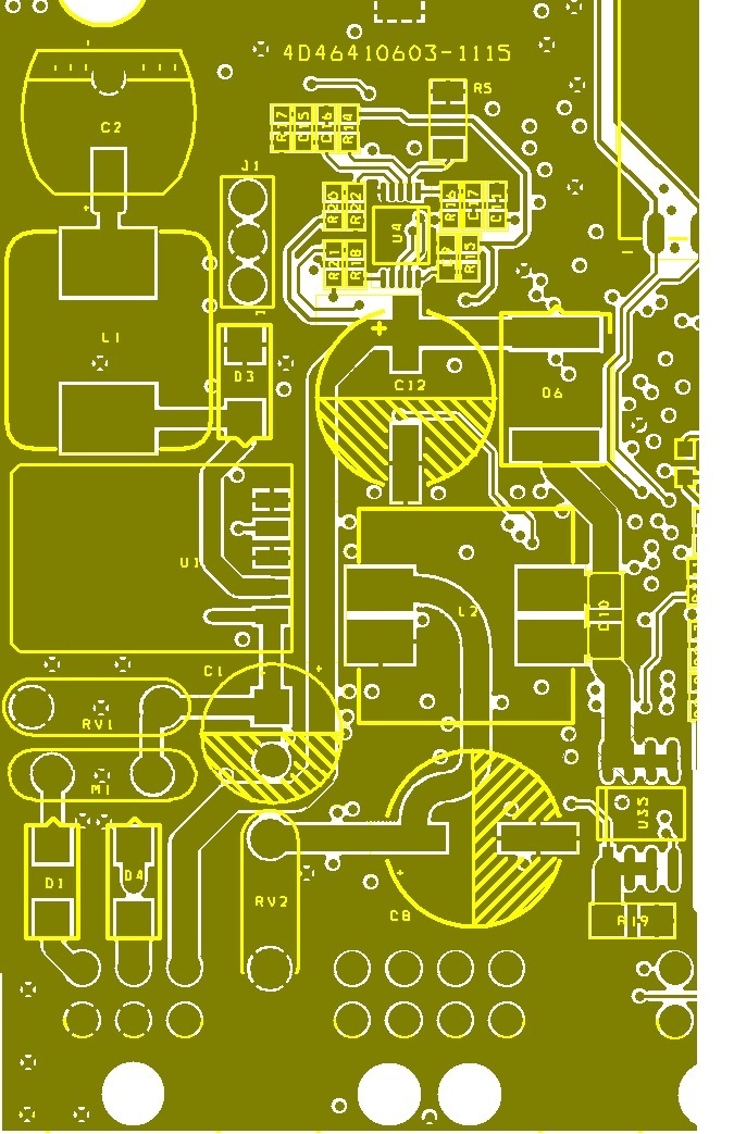
I suspect of layout, but I'd appreciate if you could have a look  at my schematic and layout to confirm that.

Here are the pictures of schematics, layout and scope (no load, 400mA and 1,5A)

Thank you
Tarcisio

  • Hi,
    I will look over your layout and schematic and get back to you tomorrow.
    Thanks,
    Murray.
  • snva461a_LM3481_sepic.pdfLM3481_sepic_layout_recommendations.pptxHi,

    I attach some documentation which might help with board layout.

    Couple of comments on the schematic and the layout:

    1. Input C is only rated at 35V this will be derated with higher VIN so I would suggest changing this to 50V

    2. I would increase your O/P C to 150uF to see if that improves the noise seen

    3. In terms of the layout the FET is placed to far away from the IC and this will cause noise.

    4. Its hard to tell from your layout how you have your VIN/PGND and AGND connected wit that in mind please look over the documentation attached.

    5. I would also suggest placing the VCC cap closer to the pin.

    Are there any specific conditions that these spikes are occurring?

    Thanks,

    Murray.

  • Hello Murray,

    1. Ok.

    2. I already was using a 150uF cap. I increased it to 330uF but the results are the same.

    3.
    4.
    5. I have changed the design. See attached bellow the new layout . I believe its better now.

    Can you take a look and make new suggestion if need another change.

    The spikes occurs whenever there are load. Any load is enough to start the spikes.

    But the greater the load, greater the spikes are.

    Thank you

  • Hi ,

    Let's first address some issues in the Schematic .

    1. Add Ceramic Capacitance at the input .Use 10UF/50V X7R  Cap.

    2. If 3A needs to be supported , for output use two  Low ESR  180uF Caps in Parallel  like '25SVPF180M with 10UF/25V Ceramic Cap at the front end .

    3. Further 4A DRQ Coupled inductor will get saturated at 9V input  and  12V@3A output . For Calculations , you can refer to 

     www.ti.com/.../snva168e.pdf 

    On the Layout :

    1.Placement of Input Capacitor. Use cermaic Cap and place it next to inductor L2 pinout  .

    2. Placement of FET . Place it Closer to inductor pinout .This will minimize the high switching current loop.

    Below is the sample Layout for your reference .

    On the measurement of Output Ripple: 

    Measure the Output ripple across the output capacitance minimizing the long ground loop of the probe .

    On the Switch node noise :

    You might want to leave the space for snubber across the diode . Initial value you can start with are 4.7 ohm and 470pF . 

    With Best Regards 

    Ambreesh