This thread has been locked.

If you have a related question, please click the "Ask a related question" button in the top right corner. The newly created question will be automatically linked to this question.

LM2734 Schematic Review

Other Parts Discussed in Thread: LM2734, LM3668

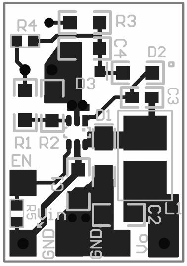
I would like to to review my LM2734 Schematic and PCB Layout to go for prototype testing.

My doubts are, Enable pin i directly connected to VIN. i think its always enabled. and  My requirements here is 5V output, 1 Amps current.the input voltage should be in 3.3 to 8V 

Please review and suggest if i need to implement something better

  • Hi ,

    You pointed out your SMPS  requirement as 3V to 8V input and 5V @ 1A output . LM2734(Buck) wont be able to regulate to 5V  output at lower voltages . This application will require a SEPIC topology . Assuming you need 8V to 5V@1A :

    1. Enable pin can be tied to Vin pin.

    2.Which device version  is chosen : X(1.6 MHz) or Y(550Khz) Version  ?

    3. On the layout:  Place C5 next to D5 and put the feedback resistance as far as possible form switch node . I will recommend you to follow the EVM Layout 

    http://www.ti.com/lit/ug/snva100a/snva100a.pdf


    With Best Regards 

    Ambreesh Tripathi 

  • Hi

    Thank you so much for your response.

    I can adjust the component placement, but actually the minimum voltage will apply from USB power, may i know minimum voltage need to apply to the regulator?

    I would like to know which version is good  X(1.6 MHz) or Y(550Khz)?

  • Hi,

    The minimum input voltage require for 5V regulation is 5.6V for Y version(550KHz) and 5.9V for X version(1.6MHz). If you are planning to power this device from USB to get 5V@1A , it wont be possible ( Vin range from USB is 4.5V to 5.5V ).More suitable option will be to use LM3668 .You can use Webench for application Schematic . 

    Ambreesh