This thread has been locked.

If you have a related question, please click the "Ask a related question" button in the top right corner. The newly created question will be automatically linked to this question.

TLV62090 - About absolute Maximum Ratings of SW pin

Guru 21045 points
Other Parts Discussed in Thread: TLV62090

Hi Team,


Our customer are evaluating TLV62090 at the following conditions.


------------------

[Conditions1]

VIN=1V

VOUT=1.5V (The voltage is applied from the outside(other power supply).)

EN=LOW (shut down)


[Q1]

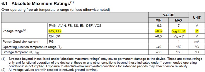
I understand that they don’t use TLV62090 at this condition because SW pin is out of absolute Maximum Ratings.

Is my understanding correct?


------------------


[Conditon2]

VIN=5V

VOUT=From 1.5V to 1.8V

EN=From Low to High


[Q2]

I understand that TLV62098 have function of pre-bias start up.

e2e.ti.com/.../1931518


So, this operation does not have any problem.

Is my understanding correct?

------------------


If you contact to below my e-mail address or let me know your e-mail address,

I can send the customer information(measurement waveform & circuit).

I’m looking forward to hearing from you.


[my e-mail address]

Kanemaru-h@clv.macnica.co.jp


Regards,

Kanemaru

  • For Q1, why does the input stay at 1V? It would usually go to 0V from leakage.

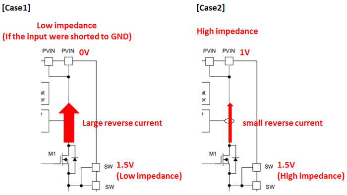
    If a voltage is present on the output, this will flow through the high side MOSFET body diode and appear on the input. This is ok so long as excessive current is not drawn. This would be the case if the input were shorted to GND, for example.

    For Q2, yes the device can start into a pre-bias as previously stated.

    If there is something special that you cannot post here, send it to me via a message in the conversation window.
  • Hi Chris-san,

    Thank you for the information.

    I will report it to our customer.

    If I have any questions, I will contact you again.

    Regards,

    Kanemaru

  • Hi Chris-san,


    Sorry again for asking you this when you are busy.

    I have one more question.

    Does this situation(it is Q1) not have any problem if the input and output are “High impedance” so the current don't flow from output to input?

    I’d greatly appreciate your verification.


    Regards,

    Kanemaru

  • Hi Kanemaru-san,

    I do not understand your question. Can you rephrase it?

    If the source which is applying the 1V and 1.5V are high impedance, then leakages on those nodes (from the system) would likely sink those voltages to 0V.
  • Hi Chris-san,


    I’m terribly sorry for confusing you.

    I understand that this device is failed by the reverse current at Case1.

    If Case2, can I use this device?


    Regards,

    Kanemaru

  • Yes, case 1 is generally prohibited and not desired. A large current will flow, which is generally not accepted in the application. The device may not fail, but this depends on the impedances in the system.

    Case 2 is ok. At DC, there will be very little current flow though the high impedances.
  • Hi Chris-san,


    Thank you for your prompt reply.

    And, I have one more question.

    How much value does the reverse current permit at Case2?

    We would like to know the upper limit level of the reverse current.

    Could you please let us know it if you have any information?


    Regards,

    Kanemaru

  • This is not specified, but a general rule is that any reverse current should remain below the current rating of the IC (3A), while the temp rise created (from the rather high forward voltage drop) should not cause the Tj to exceed the rating.
  • Hi Chris-san,

    Thank you for the information.

    I understand. Thank you very much.

    Regards,

    Kanemaru