This thread has been locked.

If you have a related question, please click the "Ask a related question" button in the top right corner. The newly created question will be automatically linked to this question.

TPS40170 SW Input damage

Other Parts Discussed in Thread: TPS40170

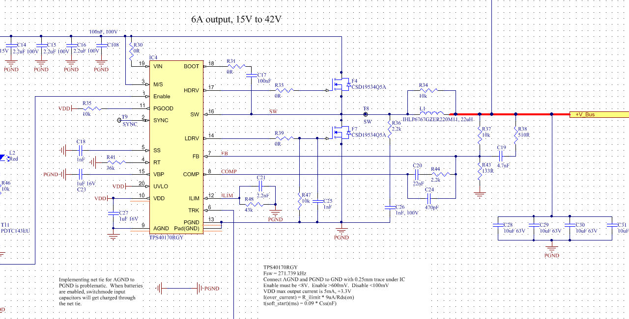
 Would appreciate some advise for preventing damage to the TPS40170 for a battery charging application.

Vin is only supplied during charging.  While not charging, the TPS40170 is not enabled.  When a battery is connected to the regulator output, the track going to the SW input blows and the TPS40170 is destroyed.  The absolute maximum for the SW input is equal to Vin.  In this scenario, Vin will be a diode drop below SW (via HS body diode).

I can prevent the damage by having a diode on the regulator output.  However the power dissipation from this is an issue for the design.  A synchronous buck design was used to minimise heat to start with.

Testing has been problematic/limited, as the damage to the PCB track makes it very difficult to replace the device.

Any alternatives would be appreciated.

  • Hi Eclipze,

    If the damage is caused by high voltage spike on SW, below methods help to reduce voltage spike.
    -Change Boot resistor R31 to several ohm.
    -Change high-side gate resistor R33 to several ohm.
    -Reduce resistor (R36) value in RC snubber. Usually the value is several ohm.

    Thanks
    Qian
  • Really appreciate your response Qian.

    I bought a development kit and re-fitted with some of my components.  It worked as expected, but I didn't try it with a battery connected on the output.  I will add a couple of ohms to the boot and high side gate resistor as you suggest.  I do suspect having SW higher than Vin has been the cause of the failures.  Using a diode on the output has prevented failures, however the heat is limiting the output current.

    I have bought some of TI's LM5050MK device implement an active diode, in an effort to reduce the heat issue.

  • Hello,

    Can you provide the .schematic . What was your application where you are using this TPS40170 IC


    Thank you
  • Bhargav, the schematic is shown in the first post.

    The last PCB design was performing quite well.  Using a boot strap series resistor of 4.7R and high side gate resistor of 1R, I have eliminated the need for a snubber at the SW.  Very clean switching.  Just limited by thermal considerations at the moment.  I do not yet have good reliability and unsure how to protect the TPS40170 from damage.  Last two boards died when the bench power supply current limited the input to the regulator.  Waiting on a new PCB revision, which includes a PI filter and a lower ESR inductor (chasing higher efficiency). I have a SMDJ40CA on the input.  VIN has a 1R series resistor.  It clamps higher than the TPS40170 maximum specification, however difficult to find one that will still run with a 48V input.

    Reliability is the main concern.  Difficult to know the exact point of failure, as catching the event (with a limited board supply) has eluded me.

  • Okay, I am starting with the schematic now, and will then move with other components (control circuit, voltage and current regulation) . For me the limitations or challenges you had building the circuit will be helpful guidelines.

    Did you uses KiCAD to design your sch and PCB .? Or any other ?

    Thank you.
  • Altium.   However you would be better off starting a new design using TI's WEBENCH design center.  You can specify your regulator requirements, choose this part and generate the schematic from this web tool.