This thread has been locked.

If you have a related question, please click the "Ask a related question" button in the top right corner. The newly created question will be automatically linked to this question.

TLV62090EVM-125: [Q] SW's frequency

Part Number: TLV62090EVM-125

Dear TI-er.

My customer was tested TLV62090EVM-125.

Test condition : Output Load is 2.5V & 1.2A.

My customer's Question

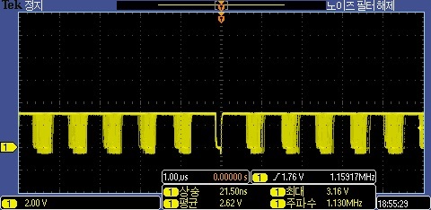
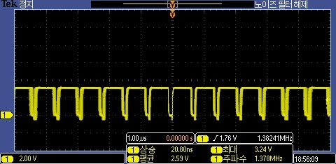
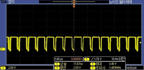
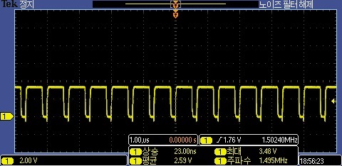
1) SW(Pin 1& 2)'s frequency is changed by input voltage. What is that ?

2)  The Frequency isn't trigerring. What is that ?

      Input voltage is 3.4V. and It is triggered.

Input voltage is 3.1V.

Input voltage is 3.2V.

Input voltage is 3.3V.

Input voltage is 3.4V.

  • Kiyoung Son,

    This is a normal behavior of the DCS-Control topology. The device is on-time controlled and runs with a switching frequency that depends on the duty cycle (VOUT/VIN). If the duty cycle becomes larger and larger (VIN decreases), the on-time becomes larger as well.The off-time is set lower to keep the switching frequency stable (see Figure 5 in the datsheet for VIN>3V).

    However from a certain point of even larger on-time (VIN decreases further), the switching frequency can't be kept and gets decreased to keep the duty cycle as needed (see Figure 5 for VIN<3V). For VOUT=2.5V, this happens at larger VIN as the customer has seen.

    In that range, the on-time is too long to keep duty cycle within the formerly given switching frequency. So the switching frequency is reduced to keep the duty cycle that is needed to get VOUT properly. This regulation mode  now sets ton cycle by cycle a bit different and looks like a frequency jitter in the plots above. This is not an unstable behavior.

    Thanks and Regards

    casc

  • Hello Kiyoung,

    Fsw changes is shown in datasheet: page 7 and 8.

    More information regarding frequency variation please find in following document:

     Is it possible to share schematic and layout?

    Best regards

    Lubomir