This thread has been locked.

If you have a related question, please click the "Ask a related question" button in the top right corner. The newly created question will be automatically linked to this question.

WEBENCH® Tools/TPS54232: Insufficient Current And Voltage Dropping With Load

Part Number: TPS54232

Tool/software: WEBENCH® Design Tools

Hello,

We used TPS54232 for a buck project based on Webench design, which on previous projects, webench was pretty accurate and now there is an issue with insufficient current when testing the circuit with load. 

The circuit outputs 5.17v which is ok but the MAX current is 250 to 300mA in 4v and less... if increasing the load, it drops even to 2v without increasing the current (Vin in this case was 13v).

Question is, why its happened? what components/ values need to be replace in this design?

I made a new webench design with the same requirements and it gave three different parameters from the last time (RCOMP=49.9K, COMP2=10PF, COUT=22UF) I changed this three instead of the basic design and it did not influenced the current...  

VIN 10.5V - 27V

VOUT 5.15V

I OUT 1.5A

Attached the schematic and the new webench design for reference.

Appreciate your Assistance!

Thank you,

8132.WebenchReportsServlet.pdf

  • in addition, when VIN=19.8V, it gives 5.3v, 300mA, not before that. and beyond VIN=

    20.5v, it starts to stress and be noisy.

    Is this forum is Active??

  • Hi
    The webench schematic should work.
    what's your L-10uH parameter? Is the current ability enough? change a smaller value with bigger current to double check.
    Could you please upload some waveform to review, such as Vout, VSW, comp, and inductor current?
    also please upload your application schematic and layout to review.

    BR,
    Yuchang
  • Hi Yuchang,

    Thank you for your reply.

    I have made a new testing for load of 5v and the max output it gave was 0.8A unstable – meaning it dropped from 5.2v to 4.2v and current in addition to the output voltage is not stable with this loads.

    As for Inductor, I am using Vishay IHLP2525CZER100M01 3A, I changed to we 7447709100 7.1A and it gave the same results and then I back to Vishay L1 and it still gave the same results.

    Attached are the waveforms pictures based on Vin=12.4v from lab power source and the voltage pins reading bellow:

    PIN1=11.45V

    PIN2=12.34V

    PIN3=2.34V

    PIN4=1.06V WITH LOAD AND 1.69V WITHOUT LOAD

    PIN5=0.68V

    PIN6=0.56V

    PIN8=5.2V.

  • Hi bar greidy,

    The PH waveform from your test is unstable.

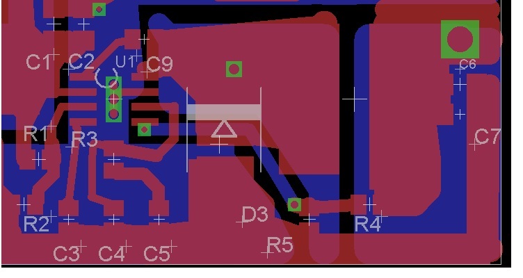
    The layout is not good, comp pin line is too close to Diode, and FB pin is too close to PH at the bottom layer, this will cause comp and FB easily be coupled switching noise, and then casue loop unstable, I suppose this cause the issue happen.

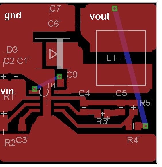
    You can refer to our EVM layout desgin or reference layout in DS, put Diode up to another side, make it away from comp and FB pin, make inductor and PH copper away from comp and VFB line, even not too close to GND pin, better place COMP RC and FB devider close to pin. and PH copper of bottom can be cancelled.

    you can check comp waveform and fb waveform to confirm the layout issue,

    And if you want to change the layout by manuual , you can refer to below picture, and then re-test it.

  • Hi Yuchang,

    Well noted and Thank you for your reply.

    Please advice if the bellow pcb will answer your suggestion for max efficiency and to solve this issue?

    Regards,

    please