This thread has been locked.

If you have a related question, please click the "Ask a related question" button in the top right corner. The newly created question will be automatically linked to this question.

TPS40170: Using Faster FETs results in gate drive oscillations.

Part Number: TPS40170
Other Parts Discussed in Thread: CSD88539ND

Dear E's,

During evaluating several different FETs for reducing switching losses, TPS40170 starts to run in hic up mode, when ever a fast FET pair is used.

Looking at slow start voltage across C611, it looks like a over current is triggered each time, because this voltage always ramps up and down like a saw tooth.

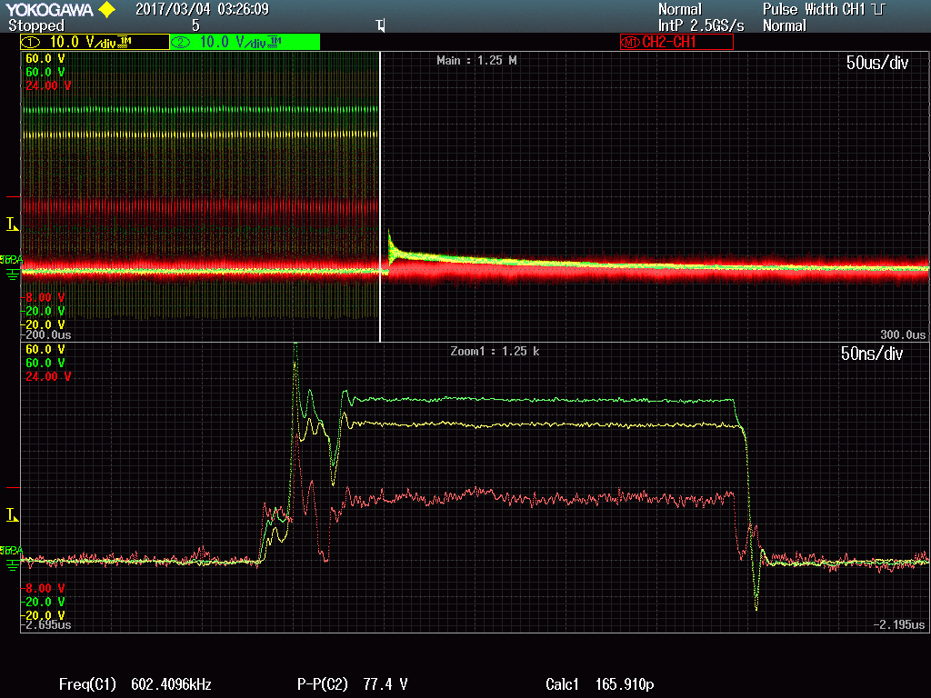
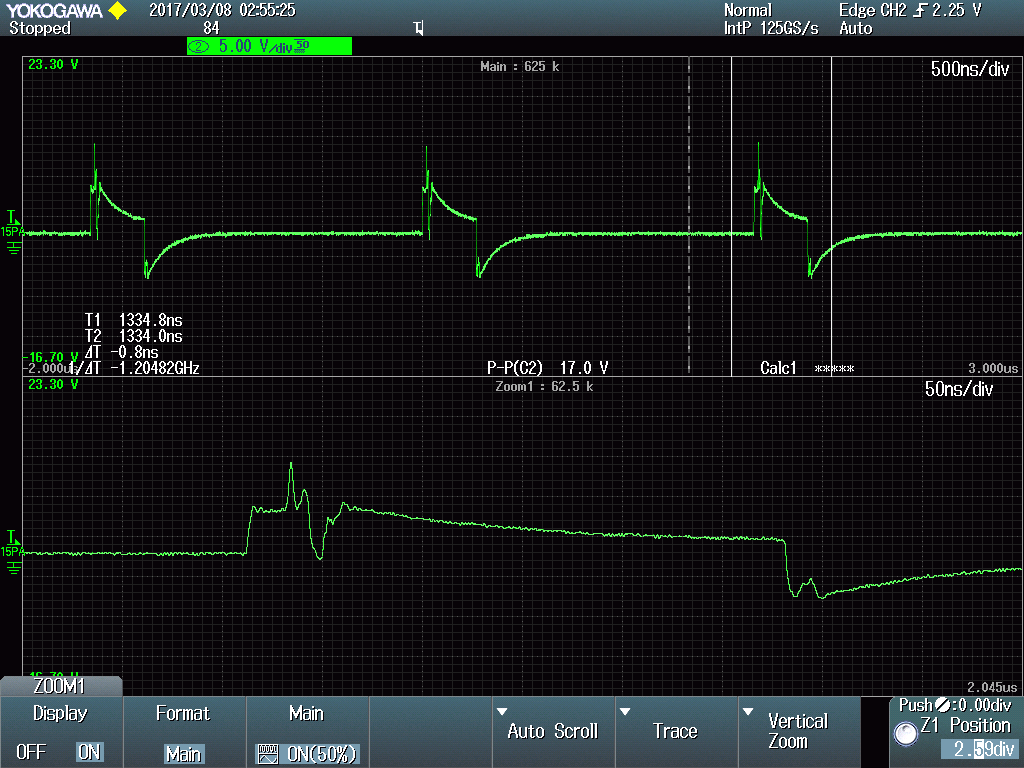
While searching for the reason, i came across a strange voltage dip in switch node voltage, which occurs just about 40ns after turn on of high side FET. This dip can be seen on high side gate drive signal as well. That confused me a bit, because it doesn't occered right at the rising edge of the switch node, but with some delay.

As ringing won't stops early enough this might be the reason for tripping the over current limit. (In threat TPS40170 blanking interval it is state to be 100ns) Thus the ringing approaches this point.

(Note over current limit is increased to Uilim = 300mV already)

Which pin of TPS40170 is susceptible to high dV/dt signals, that can actively pull the high gate low?

Sometimes it even results in some High Gate Drive oscillations within a whole Ton time. At low load conditions this doesn't occurs as dV/dt of switching node is much lower. (Due to negative inductor currents, switch node is ramped up from output inductor, and then switched on from FET. ) -> Can the high drive state be influenced by AGND bouncing or PGND bouncing?

The synchronous buck converter has following parameters.

Uin = 23V bis 44V

Uout = 5,1V

Iout = 5,5A

f = 600kHz

Best Regards,

Thomas

  • Hi Thomas,

    Due to the high dv/dt on switching node and the capacitance coupling between low-side FET drain and gate, the low-side might be turned on a little bit and cause dip on SW.

    Can you check if there is bump on low-side FET gate at the time that dip occurs at SW?

    Btw, usually a RC snubber is required on SW to lower dv/dt during high-side turn on.

    Thanks

    Qian

  • Hi Qian,

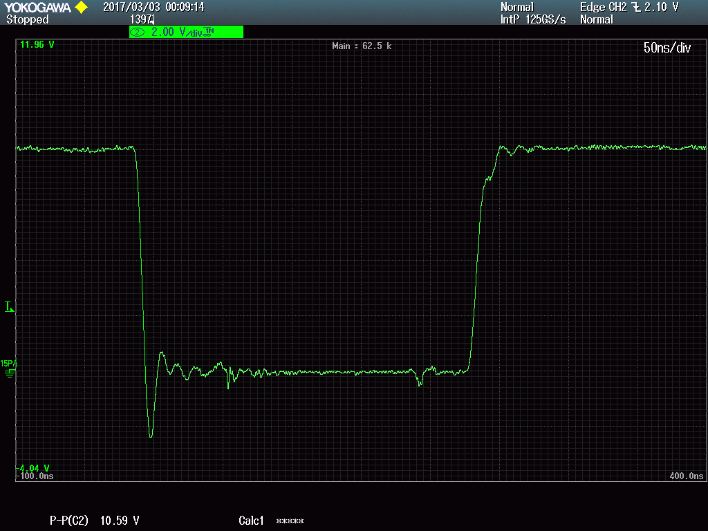
    thank you for the quick response. Yes i checked that already and couldn't find such turn on behavior at the FET pins. Here are some scope shots of gate source voltage directly at low side FET:

    By the way the Scope Shots are captured with the CSD88539ND FETs.

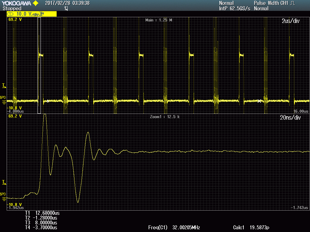
    Same measurement with the switch node voltage at Ch1, but without additional ground connection of channel 1 -> thus ringing in switch node comes from long ground return of Ch1.

    For reducing the ringing at switch node, i already added a small snubber circuit. (Csnub = 2*Coss, Rsnubb = 6ohm) That effectivly reduced the ringing time, but dV/dt was still quiet high, due to the high FET currents during switching. (When switch node starts to rise FETs are already driving high currents due to reverse recovery of low side body diode -> plateu voltage is probably quiet high)

    What is the recommended maximum dV/dt of switch node, if such a limit exists?

    Best Regards,

    Thomas

  • Hi Thomas,

    Can you find a differential probe to check the Vgs voltage of high-side FET?
    Just want to check if the dip on SW is caused by high-side Vgs.

    Thanks
    Qian
  • Hi Qian,

    Thank  you for the good hint.

    I found just a NI5191, which can only deal with up to 42Vpeak common mode range.

    First try with two voltage dividers (10kohm - 10kohm) to GND for reducing the signal levels. But that limited the bandwidth to (10kohm * 2pF -> 8 MHz) And the ringing couldn't be seen at all, just smooth curves.

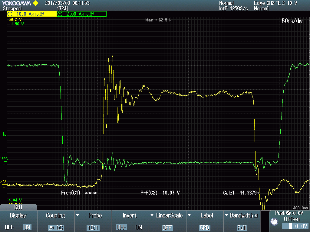
    Second run was just by let Scope-Ground float against the supply ground and only measure the differential voltage, hoping that GND-coupling between scope and supply doesn't introduces unwanted signals in interesting frequency range, but still let it be possible to measure even under 48V switching. That gives following pictures:

    For no load condition as reference, due to AC-behaviour of floating ground:

    And for full load condition:

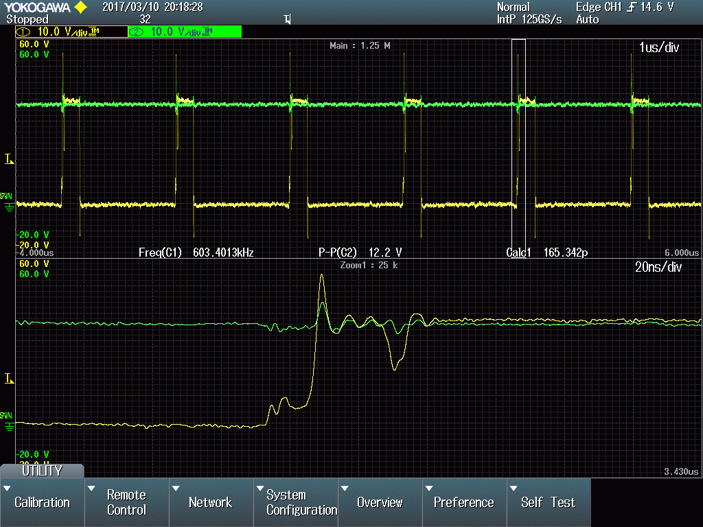
    I'm wondering which kind of parasitic inductance or capacitive coupling can push the gate drive signal that much up and pulling it down afterwards. (Even below the gate drive signal) -> Is it a layout issue or something else?.

    I couldn't determine a simple parasitic inductance as root cause for this ringing behavior.

    Schaltdurchsteuerung_HighSpeed.zip

    Layout is not perfect for now, and can be improved. e.g. by turning the FETs. But is this already the reason for high rinign on gate drive?

    Here is the case if Gate drive rings during Ton:

    Best Regards,

    Thomas

  • Hi Thomas,

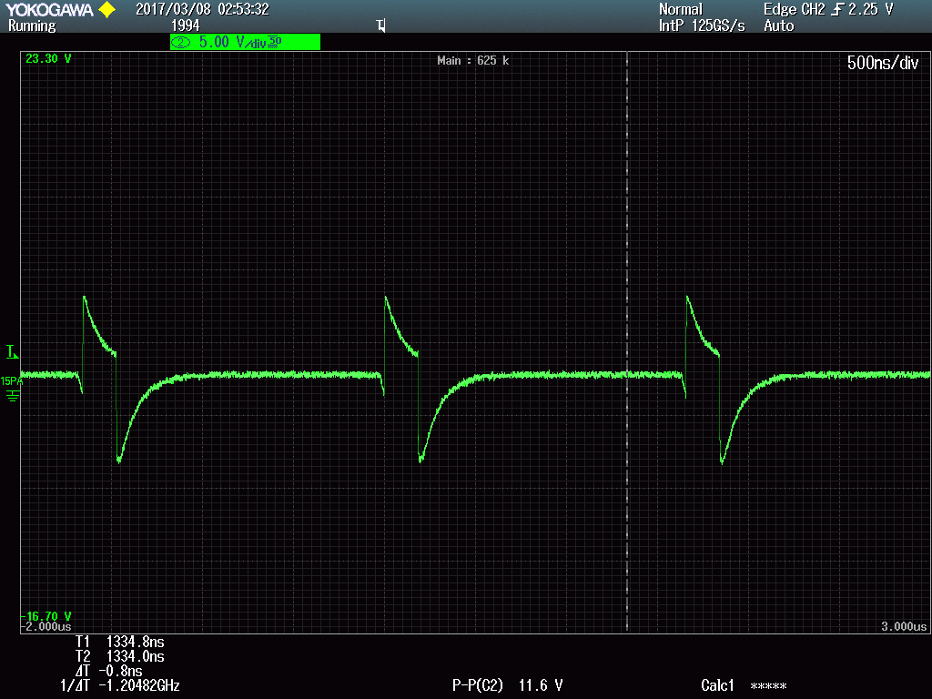
    Can you check if there is a corresponding dip on the drain pin of high-side FET?

    I see the input cap (C601 and C602) is not close to the high-side FET.

    If there is, the dip on drain pin could cause dip on gate due to the drain to gate capacitance.

    Thanks

    Qian

  • Hi Qian,


    good idea. Here is the scope shot for this.

    Best Regards,

    Thomas

  • Any updates if a too high dV/dt in Switch node can actually trigger a short turn off of high side gate drive?
  • Well it says in the data sheet on page 29:

    "8.1.2 SW Node Snubber Capacitor

    Observable voltage ringing at the SW node is caused by fast switching edges and parasitic inductance and

    capacitance. If the ringing results in excessive voltage on the SW node, or erratic operation of the converter, an

    RC snubber may be used to dampen the ringing and ensure proper operation over the full load range. See

    design example."

    So the original Apps person saw odd behavior that was managed by an R-C snubber on the switch node.

    If you have a malfunctioning board you could add an external snubber with leaded parts (keep lead length short.) as an experiment to see the impact.

  • Short conclusions after more in circuit testing:
    TPS40170 is a fine and versatile IC for voltage mode control of a synchronous buck converter.
    However my main fault at designing the circuit was the high ringing at the switch node. All scope shots below show ringing of more then 10V above the DC-input voltage level. That is too much for achieving the high performance levels the TPS40170 can provide.
    Such ringing caused degraded PSRR at low frequencies in my design, because it offsetted Vcomp by high frequency puls recitifcation.
    Or this High Side Gate Drive pull down and oscillation under very high dV/dt conditions.

    The main cause of this ringing is the parasitic inductance between high side and low side FETs. Thus must be minimized with as much effort as possible. In my layout there is a 8mm copper trace with a width of 2mm between the FETs. This is far too long and creates too much inductance.
    Reducing this length to almost none (< 1mm) , will reduce the ringing significantly. A very good layout example is the TPS40170 Eval board. (www.ti.com/.../TPS40170EVM-578

    Alternatively using the switch modules (like www.ti.com/.../power-mosfet-module-power-block.page) could even more reduce this parasitic inductance.

    Snubber Circuits and gate Resistors can make a not as good layout work at the cost of increased switching losses, however they are not the main cause and more work arounds.

    In higher voltage buck converters like here (Vin > 30V) snubber circuits have the additional drawback of hardly reducing the first ringing spike, as the switching currents due to reverse recovery and output capacitance are so high (10s of A) that the snubber must be either very large to achieve similar high currents for reducing turn on slope or it reduces just the ringing duration quiet good.

    Thanks for pointing me into the right direction.
    Best Regards,

    Thomas