This thread has been locked.

If you have a related question, please click the "Ask a related question" button in the top right corner. The newly created question will be automatically linked to this question.

tps63024: TPS63024 - About behavior when VIN=VOUT=3.3V

Guru 21045 points
Part Number: TPS63024

Hi Team,


Our customer would like to know the behavior when VIN=VOUT=3.3V.

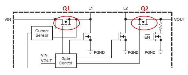
We understand that the Q1 and Q2 is ON(so Duty cycle is 100%).

Is my understanding correct?


They worry whether other internal MOSFET does not perform switching.

Could you please let us know if you have any concern?


Regards,

Kanemaru

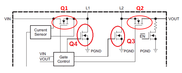
  • As described in section 9.1 of the datasheet, the two active switches (q1 and q2 ) can not be active at the same time.  This controlling method allows the converter to always keep higher efficiency, also in the buck boost region. 

    When Vin=Vout (buck-boost region), the device either operates in buck mode  (Q1 and Q3 swtiching) or boost mode (Q2 and Q4 swtiching). depending on the Buck ramp and boost ramp (Figure 3 of the datasheet). The devive can toogle between both modes when Vin is close to Vout.

    In section 9.4.1 you can find more details on how the device detects, weather to operate in buck or boost mode when Vin= Vout.

  • Hi Sabrina-san,


    Thank you for your prompt reply.

    I confirmed the following contents.


    And, I understood it as follows.

    Is my understanding correct?


    [My understanding]

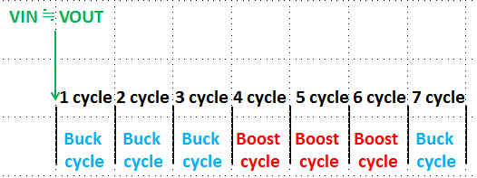
    When the input voltage is close to the output voltage;

    -First, buck cycle(so, buck mode).

    -Then, boost cycle(so, boost mode).

    -Repeats this in turn but the same mode does not follow more than 3 cycles.


    Regards,

    Kanemaru

  • This is one possible scenario of the switching behavior in the buck-boost region, It is not the only one, of course this will depend on "which of the two ramps the gmc output crosses either the Buck or the Boost stage will be initiated" 

  • Hi Sabrina-san,


    I have one more question.

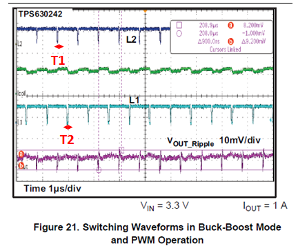
    We would like to know the minimum OFF time(T1 and T2) at VIN=VOUT.

    Could you please let us know if you have any information?


    Regards,

    Kanemaru

  • There is a minimum OFF time for the switches in this device.
    Why does the customer need the exact number? I would like to understand how critical is this information for their application before providing it.
    You can send me a private message if you do not want to disclose it on a public forum.
  • Hi Sabrina-san,


    Thank you for your reply.

    Our customer are concerned about the output voltage noise and the switching timing at VIN=VOUT.

    Therefore, they would like to know the accurate behavior (the minimum OFF time).

    *There is no need for you to guarantee this value.


    And, I have two questions.

    -Is the minimum OFF time affected by the VIN, VOUT, IOUT?

    - Are "T1" and "T2" the same time?


    Regards,

    Kanemaru