This thread has been locked.

If you have a related question, please click the "Ask a related question" button in the top right corner. The newly created question will be automatically linked to this question.

TPS65131: Problem at Negative Output - Urgent

Part Number: TPS65131

Hi,

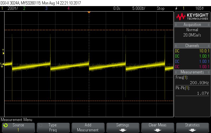
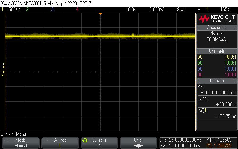
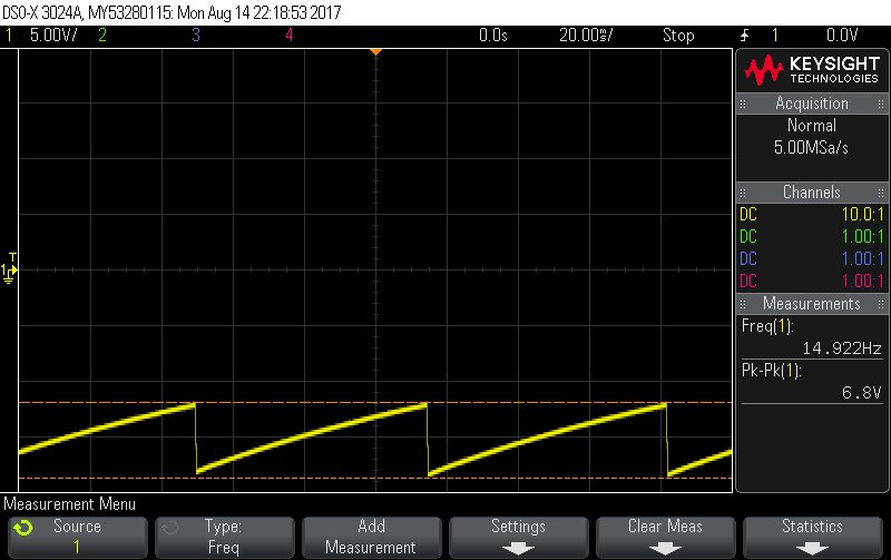
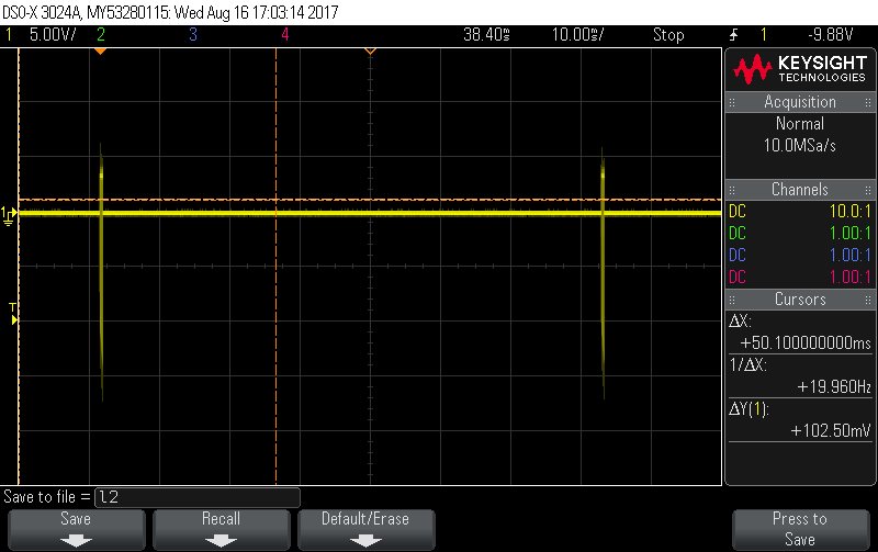
I have a problem with the negative output. Attached is the schematic (U79) and some pictures from the scope.

The scope results are with R2 = 100K and R4 = 100K as in the schematic.

Before that, by mistake, R2 was 75K giving a 18V at VPOS. So I replace it to the current value.

Is there a problem in the chip itself ?

Thanks

Noam

VREF

FBN

VOUT NEG

 IOs _ IOs.pdf

  • Hello Noam,

    Is it possible that you mixed the measurements of VREF and FBN? FBN should be around 0V and VREF should be at 1.213V.
    In your schematic PSN and PSP are connected to VIN, so you allow the device to go in power save mode. Although the ripple seems to be extremely high with more than 5V, this could be a combination of GND shift and PSN mode. Please check out if the problem is gone when connecting PSN to GND.

    I mention GND shift, because especially the connections of the components connected from CN, CP, FBN and FBP to AGND is important on this component. AGND needs to be a very clean GND directly connected to the power pad to make sure the IC is able to regulate properly. Such a high ripple on VNEG might be the result of problems with AGND.

    If you have a second board, please check if the problem there is the same. If not, it might be a good idea to exchange the IC and check the problem then and if this does not help, I would recommend to order the EVM and replace the components on the EVM with the ones you are using to check if the problem is then gone.

    Best regards,
    Brigitte
  • Brigitte Hi,

    Thank you for your support.

    I checked a second board it has the same behavior.

    Does your comment about the AGND refer to the VPOS as well, because it is stable.

    Can it be the load on the VNEG? Does it require minimal load to be stable? does changing the parallel capacitor (To R3) can help?

    BR

    Noam

  • Hello Noam,

    Please measure as well the switch node, it seems that the part is in power save mode during the time when VNEG get closer to GND.

    Did you check to connect PSN to GND? It does not look like instability, it looks like power save mode with too much ripple. So please first test if the problem is gone with disabling the PSN.

    Just to be sure, the output cap that is connected to the VNEG is a ceramic one and not a tantalum one?

    BTW, your output voltage on VNEG is set to 12V, not to 15V. So in PSN, the IC reacts correctly that it does not start switching until it falls below 12V. The question is now how often it switches before it stops again. Please check the moment when the output voltage gets to more than -18V. Is the IC just switching once? If this is the case, please check if your output capacitor is possibly populated wrong causing the energy in the inductor to charge it to such a negative voltage.
  • Brigitte Hi,

    It is a ceramic capacitor and not a Tantalum.

    Before disabling the power save mode I change R4 to give a -15V i.e. 80.5KOhm.

    Now the power is stable but on ~-18V.

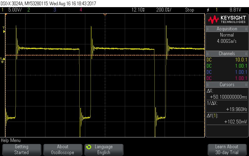
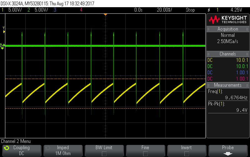
    This is what I see at the inductor L8.

    Noam

  • Brigitte Hi,

    I disabled the power save mode for both and replace R4 to be 100K as before.

    Still got the same results.

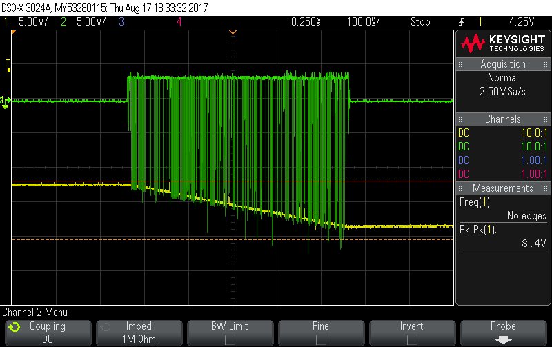
    This is what I see on L8.

    Noam

  • Brigitte Hi,

    Some inputs:

    Increasing the load (adding a resistor) make the ripple frequency getting higher.

    Changing R3 parallel capacitor make the ripple voltage to change.

    I also noticed that the voltage on VREF (Pin 17) dropped to ~0.8V. What can make it drops from 1.213 to 0.8V? Isn't it an Output?

    BR

    Noam

  • Brigitte Hi,

    Please ignore my previous post. I made a mistake and replaced the VREF bypass capacitor (220nF) to 5.8pF instead of the Feedforward capacitor of R3.

    Do you think it cause a damage to the chip?

    The situation now:

    1. VPOS is OK.

    2. VREF is OK  ~1.2V

    3. VREF capacitor is 220nF.

    4. R4 and R2 are 100K.

    5. Power save mode is disabled for both converters.

    Now there is nothing on VNEG. No switching activity on the inductor.

    I urgently need a solution.

    Thanks

    Noam

  • Brigitte Hi,

    Sorry for the flowing information but I am trying different option.

    So I used another unit with the same configuration as before:

    1. VPOS is OK.

    2. VREF is OK  ~1.2V

    3. VREF capacitor is 220nF.

    4. R4 and R2 are 100K.

    5. Power save mode is disabled for NEG converters.

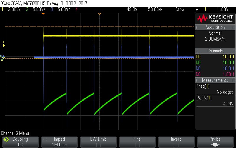
    Below is what I see at the edges of the Schottky Diode (VNEG and OUTN).

    Zoomed

  • Hello Noam,

    The bypass capacitor on VREF is essential to ensure stable operation however I do not think that removing them will damage the chip.
    Did you place back the Feedforward capacitor C349 and C348 (recommended)?

    Thanks.
    Best Regards.
    Ilona
  • Ilona Hi,

    Yes , I didn't remove it at all times. I added pictures I took from a working unit.

    Noam
  • Brigitte Hi,

    I added some snap shots from the Scope, the following are the behavior after Enable and disable.

    Enable

    Enable Zoomed

    Disable

    Any idea why the VNEG behave in save mode although I disabled it?

    Again this is very urgent and I start loosing hope.

    BR

    Noam

  • Hello Noam,

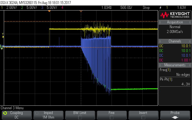
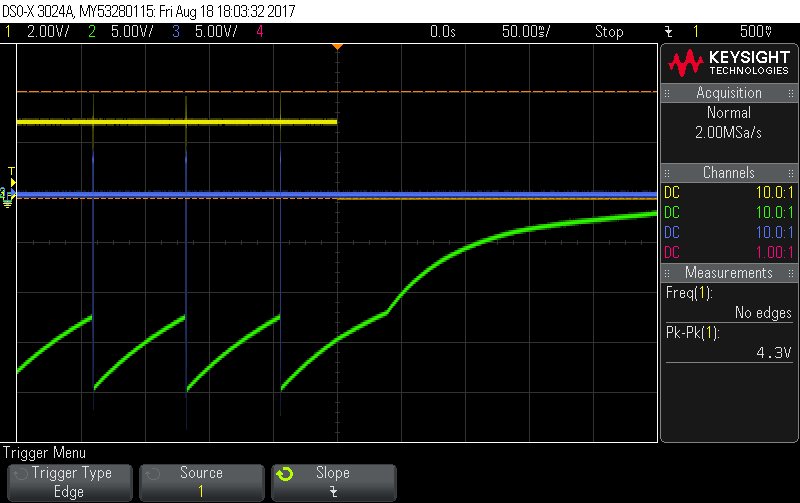
    Not sure if I got this right from the scope plots. So you see the same increased voltage ripple on VNEG in both cases? The last scope plot with 'disable' looks like it shutsdown completely for any reason (green line is discharging to gnd). Why is that?

    What you can try is to add a 50k or 100k resistor in series with the feedforward cap C349, hereby you will damp the noise coupled into VREF.

    Best Regards.

    Ilona

  • Ilona Hi,

    I disabled the power save mode and got the same results as if it was enabled. Now I am always disabling the power save mode.

    in the last pictures: Yellow = ENN, Green = VNEG, Blue = OUTN.

    The disabled picture is for disabling the negative output ENN.

    I will try the series resistor on Sunday.

    Do you have an idea why the negative output go down to ~-18V and then back to the configured value ~-12V? What do you think is wrong with the inverting converter control?

    Do you think it is noise on the VREF? As you can see the enable signal (Yellow) has a lot of noise when the switcher is working, can it cause problems?

    What should I see at the CN pin?

    There is no load on the VNEG output, can it be a problem?

    Thanks

    Noam
  • Hello Noam,

    From the first scope plots it looks like it is noise coupled into the REF/FBN pin, but I am not sure if this is due to the measurement setup (long GND loop) or the actual noise coupling on the board. If you say that your measurement technique is fully optimized the next hint for noise coupling would be layout.
    All the analog signals (ENN, VREF, FBN, CN, CP) must be routed away from the high-switching nodes (OUTN, INP) . Can you send me the layout of your schematic and I can check if this maybe gives us a hint.
    On the CN I would expect to see a DC value of ~ 700 mV.

    Best Regards.
    Ilona
  • I don't have the layer plot in a PDF format. Attached is the picture of the TOP layer. All of the components are at this layer.

    Regarding the CN, is it 0.7 V at all time or only during the Switching time? I don't have a scope picture of it but I remember that I saw some signal changes only during OUTN is switching.

    Thanks 

    Noam

    TOP.pdf

  • Ilona Hi,

    It seems the R644 is very close to the switching elements, so there might be an interference between the two.

    I will try to add the series resistor or replace the diode, D34, place with some wire stitches.

    Noam

  • Hello Noam,

    Did you try to add a resistor in series with the feedforward cap?

    Best Regards.
    Ilona
  • Ilona Hi,

    I placed the diode a little bit away from the resistor and added a 15pF in parallel to the resistor and now the power is OK.

    As you mentioned it is noise on the feedback signal that prevent the voltage locking.

    I will have to re-layout my board now.

    Thanks

    Noam

  • Ilona Hi,

    At the end increasing the parallel capacitor to ~20 pF instead of 6.8pF did the job.

    Thank you for your support.

    Noam