This thread has been locked.

If you have a related question, please click the "Ask a related question" button in the top right corner. The newly created question will be automatically linked to this question.

WEBENCH® Tools/TPS40170-Q1: Regarding bode plot & startup simulation with Webench for TPS40170-Q1

Part Number: TPS40170-Q1
Other Parts Discussed in Thread: TINA-TI, TPS40170

Tool/software: WEBENCH® Design Tools

Hi TI support,

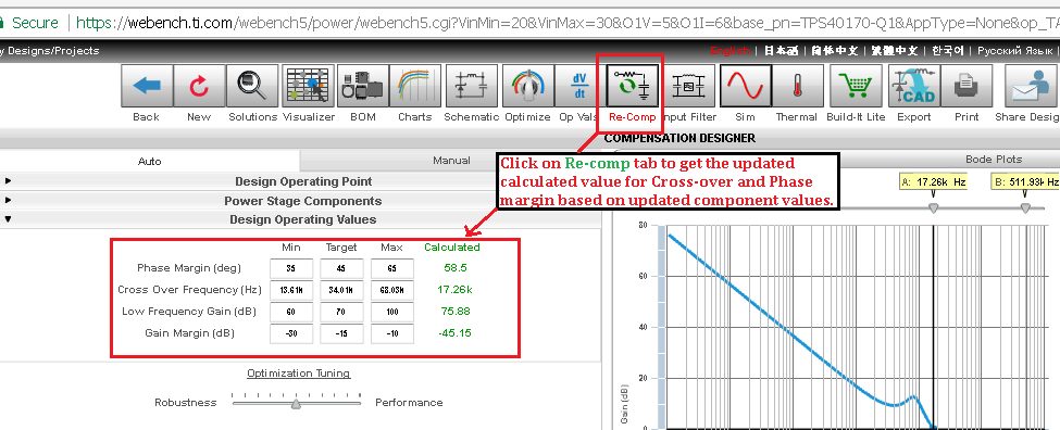
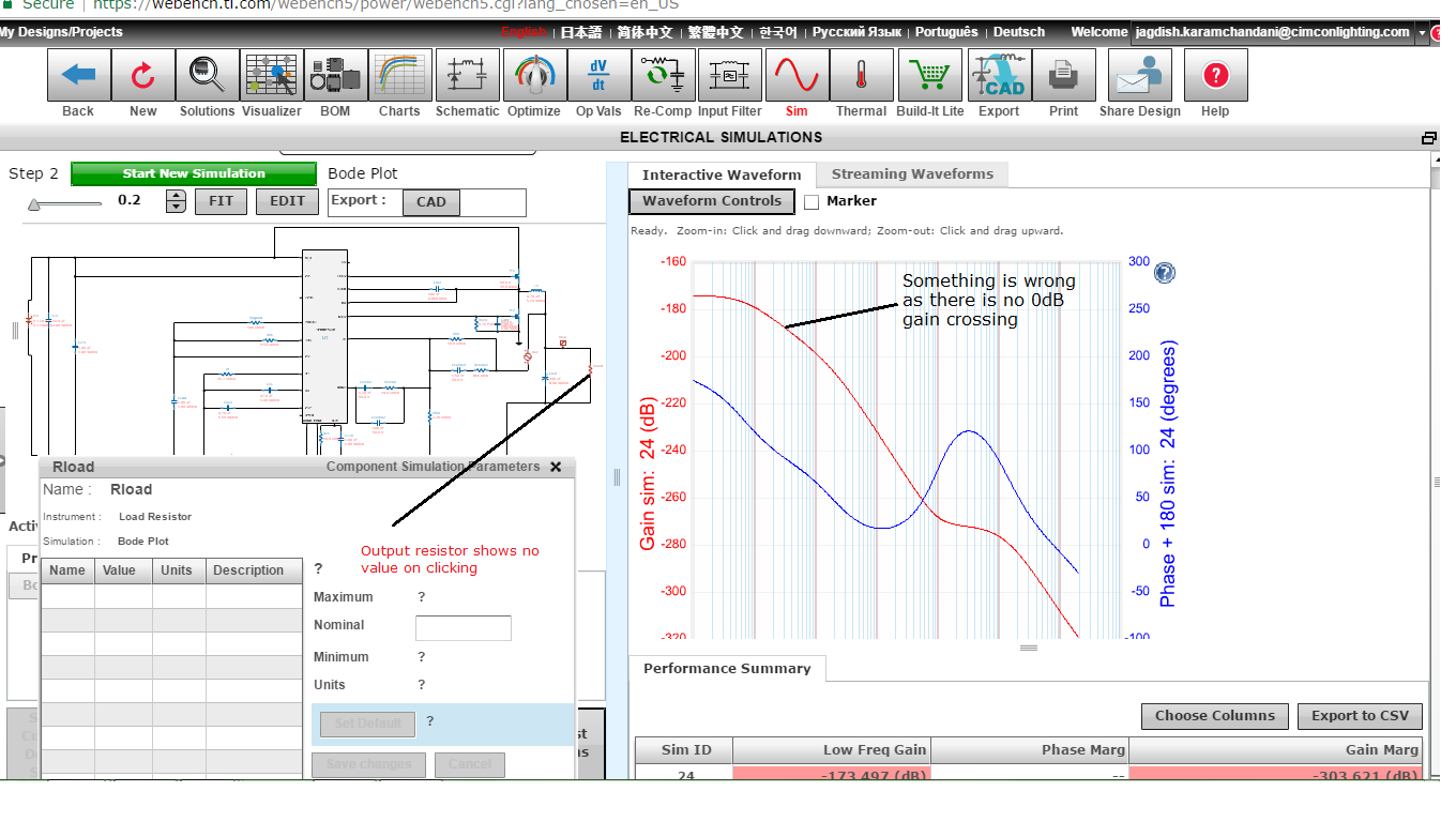
1. I generated 24V to 5V/ 6A design using Webench. Did customization of some components, used TPS40KType III tool for compensation network. Everything seems working fine with good phase margin in "Op Vals" but those things are not visible in bode plot simulation. 

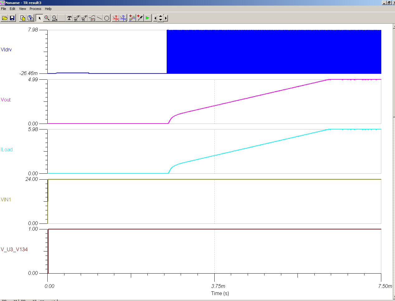
2. The other issue I face is startup simulation fails with Css=47nF. This value has been selected as per datasheet guidelines. If this value is changed to 2.2nF then startup simulation does work. Please find attached webench design generated along with this thread.

Thanks,,

jagdishwebench_design 24V-5V 6A.pdf

  • From the bode plot, the band width is the frequency where the gain curve crosses 0 dB. The phase margin the phase reading at the frequency where the gain curve crosses 0 dB. The y-axis for phase margin is at the right hand side of the plot.

    I am not sure why the Webench does not simulate with 47nF Css cap. I will leave that for the Webench support team to help you.

    -Yang
  • Hi Yang,

    Sorry for not explaining the point-1 in detail, what I meant was I can't see same phase margin (as in Op Vals) in bode plot with marker. That means bode plot & operating points mismatch in 2 of similar designs with TPS40170-Q1. This is one thing.

    The other thing which shall be considered final in such case "operating values" or bode plot.

    Thanks,

    jagdish

  • Hi Yang,

    Where you able to look into the issue. Can you please advice.

    Regards,
    jagdish
  • Hi Jagdish,

    1. Bode Simulation issue:

    Once the Design is created on Webench, the opval shows the loop calculation values such as Cross-over and phase margin based on the components values present in the created design. If the component values are modified , the OPvals calculation will still show the older calculated value. On the contrary, the spice simulation will show results based on the component values present during simulation. So if component value have been modified the spice results will get changed but Opvals will remain same.
    The solution to this problem is to use the Re-comp designer on Webench as shown in below image. The re-comp designer generates phase margin and cross-over values based on the updated design. This calculated value can be then compared with Bode simulation results on Webench. They will match closely.

    2. Startup failure issue for Css=47nF:
    We are looking into this issue. We shall notify you once it is resolved.

    Regards,

    Anurag

  • Hi Anurag,

    Thanks for your response. This is the new thing I learned today that Op Val simulates as per old components. This appears to be kind of bug. In datasheet there was mention on Loop Stability tool & hence I didn't preferred to use Re-comp designer.

    I will use the Re-comp designer & check the thing again.

    Regards,
    jagdish
  • Hi Anurag,

    Meanwhile please don't forget to update me regarding point-2 of Css=47nF.

    Regards,
    jagdish
  • Hi Anurag,

    I checked the design using Re-comp as mentioned by you but still bode plot is not working. FYI, there are still custom values of Cout, inductor & Cin. Not sure if those are interfering with bode plot or what.

    Also Ccomp2 value is near 1.33pF or so by Re-comp method while loop stability tool had this value of 100pF which is good. 1.33pF is even low compared to parasitic 3-4pF values, so don't you think design can face instability?

    Kindly advice ahead.

    Thanks,
    jagdish
  • Hi Jagdish,

    Can you please share the Design inputs( Vinmin , Vinmax , Vout , Iout and Optimiser position) for which Bode plot was not working?

    Also share the results what you are observing on Webench and the component values which are modified in the Webench schematic.

    This will help us to debug the exact cause.

    What is the loop stability tool you referred for Ccomp2 calculation?

    Regarding Startup testbench, it works fine with Css cap as 2.2nF but for Css cap of 47nF , the simulation shows Vout as zero as the we are displaying the Webench output till 1.82m. If the tstop is increased from 1.8m to a higher value, it will show that Vout starts rising  after 2m . But Increasing tstop on Webench may lead to higher simulation times. Hence I have enabled Sim-Export for the part. With Sim-Export option, the test bench can be downloaded to local machine and can be simulated i TINA-TI simulator.

    Note: The Sim Export option will be visible on TI servers by tomorrow. 

    Please visit the the following link for details on using Sim-Export : http://www.ti.com/lit/mo/slvmay6a/slvmay6a.pdf 

    Webench results with Css=47nF and tstop=1.82m

    Results for Test bench downloaded using Sim-Export option and ran in TINA-TI (with updated Css=47nF and tstop=1.82m )

    Regards,

    Anurag

  • Hi Anurag,

    Thanks for your detailed response.

    For bode plot, Vinmin=20V, Vinmax=30V, Iout=12A, Vout=3.33V, Set Freq=350KHz. Please find attached print report of the design along with this thread. Please find below screen that I see after running bode plot, gain curve starts are -ve values which can never intersect at 0db. Also notice that load resistor couldn't be changed. If you can provide email ID, I don't mind sharing login credentials where you can easily see the troubleshoot. That way it would be much better. Anyway I have changed Cout, Inductor & Cin values along with their ESRs, rest remains same.

    webench_design_855015_239_434213666.pdf

    I am using TPS40KType III Loop Stability  for calculating loop stability components which is the recommended method in datasheet.

    Css

    Thanks for bringing this out. I will check by suggested method & let you know about this.

    Regards,

    jagdish

  • Hi Jagdish,

    I created a design with Vinmin=20V, Vinmax=30V, Iout=12A, Vout=3.33V . It seems to be running fine and the Rload resistor is also present for Bode Plot.

    Could you please re-create the design again and check?

    Regards,

    Anurag

  • Hi Anurag,

    Did you used same design as I gave to you? Please confirm. I am asking because I created 2 more different designs using same TPS40170 with output of 5V & 12V but all are giving similar bode plots. In all designs same components are customized but to different values.

    Thanks,
    jagdish
  • Hi Jagdish,

    Yes, I created the design for the test conditions mentioned by you. It is ok to get custom components.

    Could you please share the design with me? My ti mail id is anurag_p@ti.com.

    Please follow the below 2 images and click on the highlighted portions for sharing the designs:

    1. Go to My Design/Projects tab on left side of page:

    After the Designs are opened. Please click on the highlighted symbol for sharing the design. Add my id to the mail list there.

    Regards,

    Anurag

  • Hi Anurag,

    Sorry for delayed response as I was out of office. Please note that I have shared all designs (with TPS40170-Q1) of 12V, 5V & 3.3V at email ID mentioned by you. Kindly note ESR for OSCON (output) capacitors is entered as per characteristics values of that component at approx 350KHz. For any query please let me know.

    Regards,
    jagdish
  • Hi Anurag,

    Any updates on this thread after sharing the designs?

    Regards,
    jagdish
  • Hi Anurag/ somebody,

    Who any of you take this thread forward & share your observations after sharing designs with you?

    Regards,
    jagdish
  • Hi TI support,

    Can anybody take this thread ahead, I think Anurag did work on this & there is no response from him.

    Regards,
    jagdish
  • Hi Jagdish,
    There was some confusion in the question about if the component is updated will it reflect in opvals. The answer is yes. Any component changes using select alternate part will get reflected in opvals table. Regarding differences between simulation and opval table, there are multiple reasons why these could be different and we are investigating this further.

    Regards,
    Gerold
  • Hi Jagdish,

    I see that you are facing issues with discrepancies between opval values and bode plot sims for this device. I suspect you are running into similar issue that we had discussed here: e2e.ti.com/.../652200 I am still working on the code fix but you might be able to reuse the workaround mentioned in the link.

    However, I would like to confirm if that is the case and the only issue you are observing. I apologize if you already shared this information before but could you please share your design using the "Share Design" button within the design and copy-pasting the link that you get using "Share with Public" option?

    Regards,
    Amod
  • Hi Jagdish,

    Did you try re-creating the design ? In case you find the same issue again, kindly share the design link here. This will help us to debug the issue faster.

    You can do so by clicking "Share Design" -> "Share with Public" -> "Get New Shareable Link" and send that link here.

    Thanks & Regards,

    Harish

  • Hi Gerold,

    Thanks for bringing this to notice that any component change will reflect in OpVals. Actually there are no differences but bode plot simulation gives absurd values where I couldn't see gain plot coming down to 0dB. Please refer figure posted in email thread.

    Regards,
    jagdish
  • Hi Amod,

    Thanks for your response. I have shared all 3 designs. The previous issue was of mismatch type while in current one I can't see proper bode plots in "Bode Simulations". It may be possible that doing workaround you suggested can do the work. Can you pls check at your end.

    Regards,
    jagdish
  • Hi Harish,

    I tried creating 2 more designs in similar way & facing same issues in all 3. I have shared all 3 designs as you have suggested.

    Thank you Gerold, Amod & Harish for your replies. Pls look & advice further.

    Regards,
    jagdish
  • Hi Jagdish,

    Thanks for the clarification. It looks like the default bode plot worked fine but when the custom components (L,Cin,Cout) were introduced the bode plot gain/phase were not proper (gain way below 0DB) Is this understanding correct? I did not get your shared design URL in your replies. If possible, please go ahead and share your design URL here. I can also try looking up your older design from December for further debugging if that is OK with you. Please let me know and we can debug this further.

    Regards,
    Amod
  • Hi Amod,

    Yes, understanding is correct. Sorry for forgetting to share the links. Pls find below links with design details.

    1. 20-30V input, 3.33V output at 12A
    webench.ti.com/.../SDP.cgi

    2. 20-30V input, 5.0V output at 6A
    webench.ti.com/.../SDP.cgi

    3. 20-30V input, 12.0V at 6A
    webench.ti.com/.../SDP.cgi

    Thanks,
    jagdish
  • Thanks Jagdish, we will look at the differences and figure out the root cause for the issue you are observing.

    Regards,
    Amod
  • Hi Jagdish,

    Thanks for your patience.

    In all the 3 shared design, we found that Rload value was not getting picked. This is the reason why gain was below 0dB

    I tried re-creating your design [20-30V input, 3.33V output at 12A] with the compensation  components same as your design.

    The simulation ran fine with Gain plot starting above 80db. Also the thing to note here is Rload value got reflected in the design.

    Below is the link for the design [20-30V input, 3.33V output at 12A] FYR.

    Design-1[20-30V input, 3.33V output at 12A]

    Could you please re-create fresh [Click here] design for the same condition & let us know following observations ?

    1. Is the Rload value in the schematic getting reflected before editing/customising your design ?

    2. After editing the components, is the Rload value getting reflected properly in the schematic ?

    3. If the issue is being observed in pt 2, kindly let us know the steps followed in editing the components ?

    Best Regards,

    Harish

  • Hi Jagdish,

    Below is the snapshot highlighting Rload value. Just hover over the component to see its value.

    Thanks & Regards,

    Harish

  • Hi Harish,

    I checked recreating design preliminary & seems working. I shall check all designs thoroughly again & let you know the issue if found any. Thanks to all for your help.

    Regards,
    jagdish
  • Hi Jagdish,

    Thanks for re-creating the designs. I have created the design for 3 cases with the components selection same as your design. Below are the links for the same.

    1. 20-30V input, 3.33V output at 12A: Design-1[20-30V input, 3.33V output at 12A]

    2. 20-30V input, 5V output at 6A: Design-2 [20-30V input, 5V output at 6A]

    3. 20-30V input, 12V output at 6A: Design-3 [20-30V input, 12V output at 6A]

    Best Regards,

    Harish

  • Hi Harish,

    Thanks, I shall check those & come back to you if any issue.

    Regards,
    jagdsih