This thread has been locked.

If you have a related question, please click the "Ask a related question" button in the top right corner. The newly created question will be automatically linked to this question.

TPS55340: doesn't boost after activating ENABLE pin

Part Number: TPS55340

Hello:


We are using TPS55340. Our board is working OK but if the voltage down to 0,2v at PIN EN the system doesn’t boost, that’s right. A time after, if the voltage at pin EN raise again up to 1,3v the system doesn’t boost anymore. We used webench tool and excel file (TPS55340 boost design calculator) and the result is the same. Does anyone have an idea what is happening?


  • Are you sure EN voltage is higher than 1.3V? if it is higher than 1.3V, it can startup. don't set it just at 1.3V, because due to lot to lot differnce, some part need EN>=1.3V to start up successfully.
  • Hi Helen

    yes, I'm sure. We tested removing R218 and populating a 20K pull-up just to have PIN EN with fixed +24v. Still doesn't start-up.

    Thank you

    Antonio

  • What is the EN frequency? Are you sure the IC is still OK and not damaged?  Please remove the Vin and then add Vin back  again to check whether the IC could startup successfully.

  • Hello Helen

    answering your questions:

    What is the EN frequency?


    It has a ON/OFF signal only use in few times.


    Are you sure the IC is still OK and not damaged? 


    I don’t know, it is the behavior in this pcb and other 3, but the question is Why a good pcb turns to this behavior?


    Please remove the Vin and then add Vin back  again to check whether the IC could startup successfully.


    Yes, if I remove the Vin the IC startup correctly until activate EN signal

    Thanks

    Antonio.

  • Thanks for the informaiton. Did you try the 1.5V-1.8V EN volatge instead of the 1.3V? Will it still have the same problem? I'll check it in the lab, what is the EN signal rise up slew rate in your experiment? I'll try to enable and disable the IC with EN on/off frequency at 200 HZ to check the perormance.
  • will give the feedback to you next week!
  • I just test on the EVM board with Vin always on and EN rise up to 1.2V to enable the IC, then EN drop to 0.8V disable the IC then rise up to the 1.2V enable the IC again, I tried many times, it is OK .
    I can't check the parameter on your sch as it is vague. COuld you make the sch clear and send to me again? there's must have something wrong with the parameter, did you test the EN voltage with the EN control volatge at the same time? if the VEN>1.2V, this problem shouldn't happen.
  • Hi Helen


    • Yes, I tried to connect EN pin through a 20K resistor to +24V, and didn’t work.

    • I measured the rise up in EN signal and it was <2uS, but what will be the point if that circuit doesn’t work?

    • No, I don’t try to enable/disable with 200Hz because for my real situation I only have 1 enable or two for each power on.

    thank you

    antonio

  • I'll double check in the lab. could you please make the EN rise time to a slower rate to try again, like 100us. I'll upadte the result to you tomorrow!
  • Hi Helen

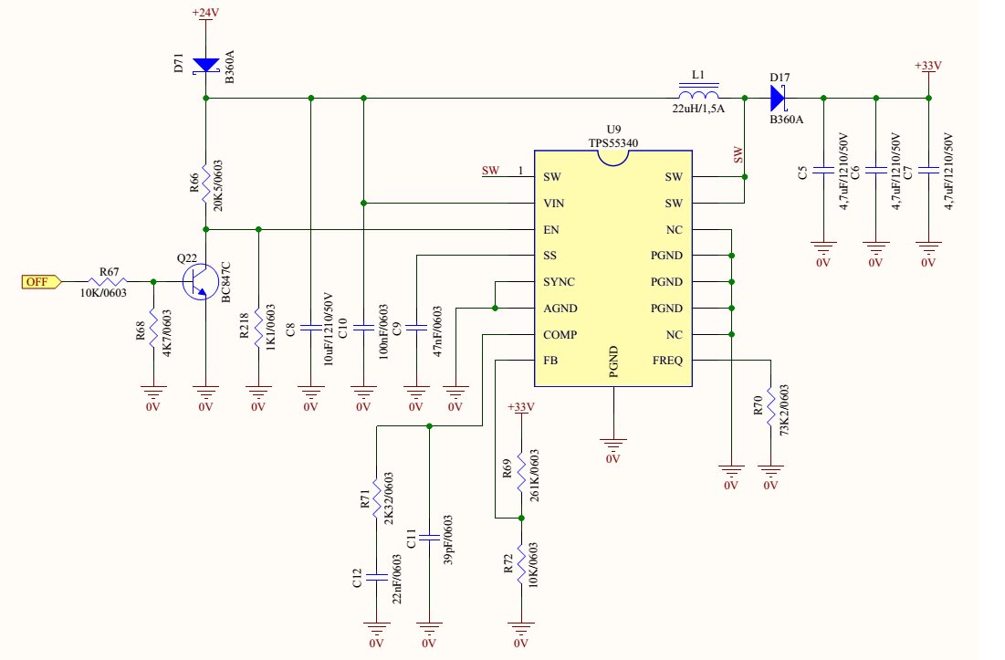
    we will try. In the meantime  attached a new sch in better resolution. I hope you could find anything that explain this problem.

    thank you.

    Antonio

  • Thanks for the sch, I'll reply you tomorrow!
  • 1. remove Q22, then change r218 to 10k. then try again.

    2. if still can't startup, then test the voltage on the EN pin.  make sure this pin is connected well.

    I tested in the lab with 50ns-100us slew rate, the EN signal can control the IC's on/off successfully.

  • Helen

    thank you very much for your help. Customer will test your recomendations. In the meantime:

    We substitute a broken TPS55340 with a new device and we did the following tests removing R218 to get more than 1,3v in PIN EN. We mounted 3 different configurations:


    1. Original configuration:

    – R70= 73K2.

    – R71= 2K23

    – C12= 22K

    – C9= 47K

    – C11= 39p

    Behavior is always good, boost up to 33v, even with 1hz square signal in PIN EN.


    1. Excel values configuration:

    – R70= 124K.

    – R71= 2K94

    – C12= 68K

    – C9= 47K

    – C11= 270p

    Behavior is always good, boost up to 33v, even with 1hz square signal in PIN EN.


    1. Webench values configuration.

    – R70= 60.4K.

    – R71= 3K32

    – C12= 68K

    – C9= 22K

    – C11= open


    Behavior is always good, boost up to 33v, even with 1hz square signal in PIN EN.

    Voltage in PIN EN is always over 26v.

    Voltage in PIN COMP is always over 1.2v.

    We all these configurations working OK we deduct that the problem was the chip (TPS55340). Why this device is broken after operating in field?

    What’s the best configuration we described above?

    antonio

  • The fail rate of TPS55340 is very very low, I think maybe because of the wrong conneciton and wrong sequence.
    What is the Vin, Io in your applicaiton? so that I can calculate the parameter.
  • Hellen

    I don't have yet Vin value. In the meantime. Following comments of my customer:

    If I remove Q22, I couldn’t control En signal and I need to control it. If I never turn off En signal, the Ic works fine but I want to control it.

    I don’t know Why when I turn off/on EN signal the IC don’t work again until I remove +24V. That’s the problem I have.

    Did you revise the sch? All values are correct?

    Antonio

  • Helen

    At the begining we thought on that a wrong connection but we have reviewed all the manufacturing documentación and we haven’t found anything wrong, moreover we start to sold with 35%pb Sn at least and the problem keep go on.

    The Vin for my application, are between 24Vdc and 28Vdc, the Vout that we need is 33V and the Iout almost 1A.

    thanks
    Antonio
  • Did you check the wrong part in detailed, which pin is damaged?
  • And totally how many part damaged, is the damagged part act in the same way? is the same pin damaged? which pin? And I need to check your layout.
  • Helen

    we are in the phase of applying a Failure Analysis.
  • So you have send the failure IC to the TI office right?

  • not yet sent. We started this week the bureaucratic process to send pieces for failure analysis. It's long.

    antonio

  • Got it. The failure analysis result can help us determine over current or over voltage. What about your layout and what about the thermal , did you test the SW spike? if the layout is not good, the IC will be very hot and the SW spike will be very high.
  • Hi Helen:

    I'm working with Antonio, and he asked to me for reply your questions. I attached the pcb desing, if have any question tell me and I answer ASAP. Also, I gonna to compare the wrong IC with another one, through measure the impedance between pin 6 and the rest of them, and between pin 11 and the rest of them; If I detect something strange I tell you.

    Thanks for your help, Regards

    TPS55340.zip

  • Hi Helen:
    There are the impedancies measures in two TPS55340:

    Damaged

    6-1 273K
    6-2 246K
    6-3 571K
    6-4 231K
    6-5 247K
    6-7 258K
    6-8 255K
    6-9 266K
    6-10 318K
    6-11 2.36R
    6-14 OL
    6-15 270K
    6-TPW 10M

    New

    6-1 281K
    6-2 281K
    6-3 566K
    6-4 230K
    6-5 247K
    6-7 258K
    6-8 259K
    6-9 275K
    6-10 329K
    6-11 2.17R
    6-14 OL
    6-15 288K
    6-TPW 6M

    Regards
  • The impedance of the 'damaged' part is OK, no obvious problem.

    Coulld you please solder the 'damaged' IC to the good pcb board to check whether the IC is reallly damaged or not?

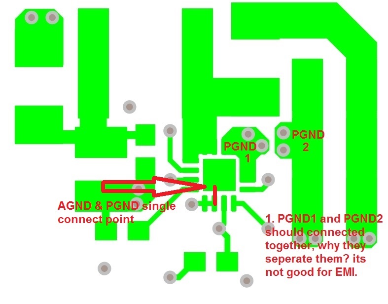
  • The layout is really bad, it seems that they mixed the AGND and the PGND together. I put the suggHelen suggestion.zipestion in the attached file. Please check it.

  • Hi Helen:

    I saw your recomendations, and yesterday when I saw your post requesting the layout, I started to review our layout and comparing it with the example in the datasheet. I realized that the connections in the top layer wasn't do it and I wrote in my book to improve in a future redesing.

    I want to ask you a few questions:

    If we do this changes that problem won't happen in the future?

    Are you completly sure, if we change the layout the problem will be gone forever?

    When we redesing the board, could I send you the new layout for a review?

    We don't have to connect PGND and AGND on internal layers, correct?

    We have to create a thermal plane on internal layers to radiate IC heat, but this plane don't have to connect with AGND or PGND, only with thermal pad throuhg vias, correct?

    We could try to change in an actual PCB the layout with your recomendations, Do a damaged IC works well again? what do you think?

    Regards

  • Hi Helen:

    I had sold the damaged IC in a good pcb board, and it doesn't boost. I did that three times, with three diferents IC and three diferents boards but nothing change the IC doesn't boost.

    Regards
  • Thanks for the test. Please apply for a TPS55340 EVM, then sold the 'damaged' IC on that EVM board again. If the reason is  caused by the poor layout, then sold the damaged IC on it  helps.

    If still doesn't work, then please send the damaged IC to the TI office ASAP.

    The current layout is really poor. there will have EMI problem, this  is why I suspect the problem may caused by the layout. So whether the problem can be solved or not, please change the layout.

  • As what I suggested, please connect the PGND and the AGND at the top layer. Pour the PGND at the top layer, inner layer. Pour the AGND at the bottom since all the control part component at the bottom layer.

    Please check the TPS55340 EVM UG for referecne.

  • Hi Helen:

    On next monday, I'll soler the damaged IC on the EVM. I still have a few questions more:

    - Could you revise the SCH attached in a post before? Are all values correct for 33 Vout and 1A Iout?

    - I attached the solder temperature curve which we solder this IC by reflow system. Is that correct?

    - I attached the schematic BOM, if you need it.

    Have a nice weekend

    Best Regards

  • Could you please share the project inforamtion to me first.  Like end equipment, volume, MP date.  My email address helen-chen@ti.com

  • I’m a contractor, hired by MP to try and help them with their boost converter. They have shipped me several of their PCBs, both non-working and working, and I’ve seen all of the same issues that you, Antonio and Juan discussed. I’ve done extensive startup and shutdown testing as well as cycling of the EN pin with a signal generator, and I haven’t seen any waveforms that look like they could damage the IC.

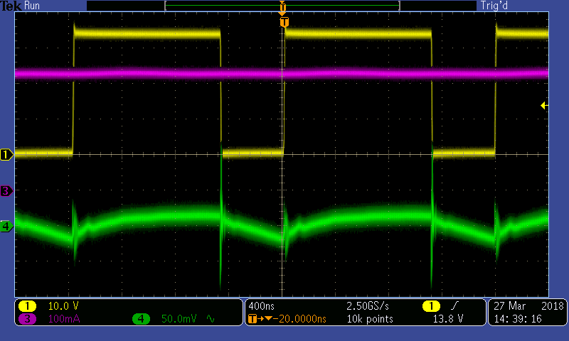
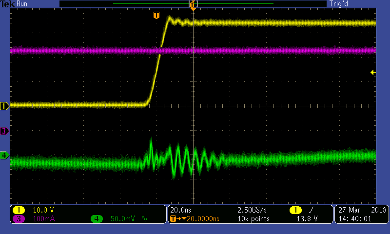
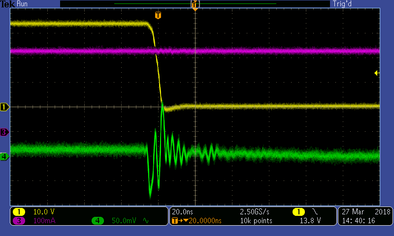
    At the end of the chain you were discussing the PCB layout, noting that connection of the AGND, PGND and PowerPAD goes through vias to internal layers instead of connecting on the top layer (where the IC is.) I took one of the working boards and put in some low-inductance test fixtures:

    While I agree that the layout could be improved, the waveforms I see don’t look bad. These were taken at the maximum output current of 330 mA.

         I noticed that you recommended trying different slew rates for the voltage at the EN pin, and that you tested that on a TPS55340 EVM. Is it possible that the added inductance of the vias between the AGND pin and the PowerPAD are causing a latchup in the IC? Since this happens during shutdown, I suppose a fast, negative transient voltage could exist between AGND and the PowerPAD. One thing I did find was that on some of the damaged TPS55340 ICs, if the EN pin was pulled to 24V via the 20k resistor (R66) upon startup, then the TPS would start switching again.

           Many thanks,

    Chris Richardson

  • Do you mean if the EN pin pulled to 24V via the 20k resistor (R66), the the IC can work normally? everything is oK?
    We need to analysis the root cause of damage per damaged IC, a long time passed, did your side ever send out the damaged IC to the TI office?
  • Hi Helen,

          My customer sent me three boards on which the TPS55340 was not responding to the EN pin signal. First I checked to make sure that the EN pin voltage was always above 1.3V, and it was. Then I removed R128, the bottom divider resistor, and applied a voltage to the EN pin with a lab supply. None of the TPS55340's turned on, even when I applied the full 24V (equal to the input voltage). However one of the boards did turn on if I powered it on with R66 in place but R128. This led me to believe that the slew rate was important.

           I will check to see if my customer has sent in any damaged parts.

    Thanks,

    Chris

  • Actually, slew rate is not so critical . I'm wonder they may met some ESD problem during production. poor layout is not a key factor of the ESD damage, but it will be more easy to trigger the ESD issue is the layout is poor.
  • Hi Helen,
    So far I have recommended that they test a small capacitance (10 nF) in parallel with a small schottky diode, both in as tight a loop as possible from the EN pin to the AGND pin. The idea is to limit any negative voltage transients on the EN pin. Would you recommend trying an ESD suppression device - TVS or similar - instead of the schottky?
    Thanks,
    Chris
  • Hi again,

    I have another data point to add: if I remove all the components connected to the EN pin and drive it with a signal generator, then it turns the IC on and off as expected. However, if I reduce the logic low of the signal generator output to below zero by more than about 0.4V (logic low of -0.4V or more) than on the subsequent rise to above +1.3V the IC does not turn on. The IC does recover if I bring the logic low back above -0.4V. So far I have not been able to permanently block the IC this way, and clearly applying negative voltages is not good - but it does tell us that a negative voltage on the EN pin can inhibit the next command to turn on.
    Thanks,

    Chris
  • ESD is mainly caused by the production, if the production enviroment is not good, then the IC is easy to be damaged during pick up, soldering, testing.....

    Add a 10nF cap near the EN pin can help this issue, but can't totally solve the issue if it is truly damaged because of ESD. They  shoulld check the production enviroment ...

    So the damaged IC is really important for us to determine the root cause.