This thread has been locked.

If you have a related question, please click the "Ask a related question" button in the top right corner. The newly created question will be automatically linked to this question.

TPS65262-1: Blown IC

Part Number: TPS65262-1

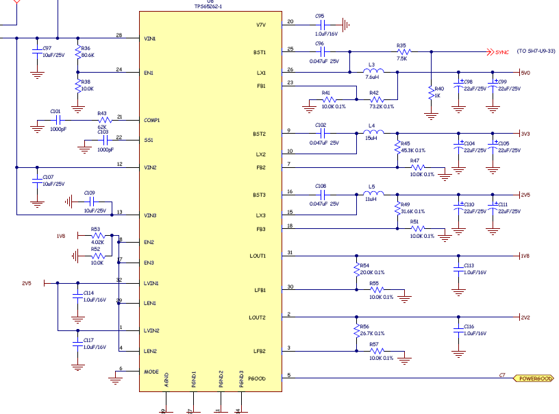
I seem to be up against a brick wall.  I have a design using a TPS65262-1

   Input 12 V

   Out1 5V

   Out 2 3.3V

   Out 3 2.5 V

   Lin 1 1.8 V

   Lin 2 2.2 V

The 5 Volt is enabled immediately (if input is above a set minimum).  The others come up after a derived 1.8 V as part of a power sequencing for a Zynq.

There are two first article PCBs in existence.  Between the two, we have blown four of these ICs, and I don't have a clue as to why.  The boards have been in use for a month or two in development labs, so its not like they always blow or have a design error.  When the first one blew, I blamed the lab supply that was providing the 12 V.  It is known to generate an overvoltage spike sometimes when the AC  switch is shut off.  But the next two failures weren't even using that supply, and the most recent failure occurred when the DC was first connected, the PS wasn't being turned on or off.  As an added protection, a 12 V TVS was placed across the input before the most recent failure occurred.

The failures are all the same.  When the 12 V power is applied, the circuit only draws about 20 MA.  V7V has the expected 6.3 V on it, but all five of the outputs are 0 or only a few mv.  Normal power up draws about 200 ma from the 12 V supply and generates the voltages mentioned above.

The exact extent and nature of the failure isn't known, because without the 5 V output (out 1) the secondary regulator has no input, and without it generating 1.8 V, the other outputs wouldn't be enabled.  So it is possible Out 2 and 3 and the linear regulators are fine, but it is known for sure that Out 1 is not functioning.

I am at a total loss as to what is causing these occasional failures.  They occur either during the previous power down, during unpowered handling, or at the moment of power up.  The last one occurred with nothing else attached to the board, except an SMA cable delivering a 7500 Hz sine wave (1 V p-p) to another part of the board.  I just don't have a model for overvoltage, stray voltage, an ESD issue or anything else.  The input has 30 uf of X7R capacitance and a TVS diode across it, which should be robust against just about anything less than a connection to AC power.

Are there any known vulnerabilities I should be designing around or protecting against?  Is there some way the secondary SMPS could spike the 5 V output and damage the FETS? (there is no other voltage source, and the 5V line has at least 75 uf of ceramic capacitors).

Here is the schematic of how the IC is used.  Not shown is the 12 V input coming in the upper left corner, and an SMBJ12A TVS diode from there to ground.

  • Hi, Wilton

    From the schematic, i find a design issue:

    The EN2, EN3, LEN1, LEN2 pin are not enabled correctly.

    After 12V power on, the Buck3 cannot be enabled, so there is no 2.5V output, --> the LDO1 is no power, there is no 1.8V output, --> without 1.8V, the Buck3 cannot be enabled, so there is no 2.5V output all the time. --> it is a dead loop.

    Work around:

    Floating EN2, EN3, LEN1, LEN2 pin. --> remove R52 and R53.

    The EN2, EN3, LEN1, LEN2 pin has pullup current, when power on, they will be pull high.

    After that, please test again.

  • Unfortunately that is not the problem.  There was a mistake on the schematic from the CAD tech.  Pin 31 should not be labeled 1V8, it should be labeled 1V8A.  1V8 is on a different sheet.

    The power up sequence is as follows:

    1.  En1 turns on Out 1, the 5 Volt output.  This powers a secondary regulator which generates 1V0, 1V8 and 1V2

    2.  The secondary regulator turns on 1V0 (and 1V2) in response to receiving 5V power.

    3.  The secondary regulator then turns on 1V8 in response to seeing 1V0

    4.  The presence of 1V8 turns on 3V3, 2V5, 1V8A and 2V2 and 2V5 supplies power to 1V8A and 2V2

    So with that misunderstanding corrected, let's make another try at the underlying problem.  The assemblers gave me back the board today with a new TPS65262-1 on it.  I connected a PS and it seemed to start properly.  I shut the lab supply off, connected USB and JTAG to the board, turned it back on and once again the TPS65262-1 is not generating 5V.  This is the fifth failure so far.  Like before V7V output is fine, but no 5V0.

    My assistant just tried to duplicate this on the other board we have.  The board was working (has been working for weeks).  He removed the connector (J5 which provides +12 power on pin 2; pin 1 is not used; ground return to the lab supply is via another connector which he did not touch) powering the board and re-connected it.  About 15 tries and the TPS65262-1 on his board blew.

    There were no other changes to the board, only the +12 input removed and applied. The power source was a linear lab  supply which remained on the whole time.  Admittedly this is an abrupt test, as the lab supply has a few thousand uf of output capacitance and the board has 30 uf of input capacitance that needs to be charged.  But I don't see how that could blow the IC, particularly as we have an SMBJ12A on the board  from +12 input to ground.

  • Hi, Wilton

    It looks the power sequence is correct.

    1. When you disconnect the USB and JTAG, power on again, could the buck1(5V) resume to work?

     Is IC damaged?

    Please check the LX1 pin whether shorted to GND.

    And check the LX1 pin whether shorted to VIN1 pin.


    2. It looks the problem lies in buck1(5V).
    Could you probe the SS1 and LX1 waveforms on issue board when no 5V output? 

    3. Please check the Vin1 cap(C97) layout, it should placed close to VIN1 pin.

    Could you send me the layout for review?


    BTW, In TI's reference design, recommend SS1 cap =10nF, but in your schematic, the SS1 cap is 1nF, it is too small, could you change it to 10nF and test again?

  • 1.  Removing USB and JTAG does not solve the problem.  The IC is damaged.  Yes. Definitely.  We've replaced five of them over this issue, in development.  There are no shorts on the board involving LX1 pin.  In several of the five, they have been running successfully for days and then one power on, they fail.  We can't tell of the failure is during power on, or during the previous power off.

    2.  Yes, I can confirm it is in buck1.  I removed the inductor and powered the 5 V net externally and all the other outputs work as expected.

    Probing the waveforms revealed quite a different story than I had expected.  First off, SS1 has 100 mv square wave, high for 0.4 ms repeating every 15 ms.  (Those numbers relate to the next part).

    Probing LX1 reveals a nice square wave from 0 to 12 volts that is high for 60 ns.  It repeats every 1.7 us.  There are bursts of those that last 0.44 ms and the bursts repeat every 15 ms.  Clearly the LX1 switch is switching.  But it also is in what would appear to be an overcurrent mode or something that is causing it to run in bursts.  Also, I would not have expected the SS1 pin to behave the way it is.

    3.  The routing of C97 seems reasonable.  There are multiple ground plane layers under the IC and components.  Some parts are on the top (where the IC is) and some are on the bottom.  C97 is on the back, about 1/4 inch from the pin and with a via to the ground plane.  The output capacitors and the grounds on U8 are all connected quite directly to the plane with vias.  I can send you the layout if you can read Altium files, or I could get the CAD department to make Gerbers or a pdf of the layers.  This is an 8 layer board, although in this area, most traces are top or bottom, and most of the mid layers are either ground planes or segmented power planes.  I'm a senior level engineer, and I signed off on the layout.  I didn't see any problems with it.

    I'm wondering about the role of the SS1 cap.  I see the 10 nF in the reference design, but I calculated 1 nF to give about 100 ms startup time, which seemed appropriate for this design.  Maybe that is too demanding on inrush current?  I don't know, but I wouldn't have thought so.  I don't have to have that fast a startup, but it doesn't seem unreasonable.

    Thanks for the input.  I look forward to your response on what I observed, particularly the burst mode and what (apparently permanent change in the IC) might be causing it and what might be triggering that.

     P.S.:  I looked at the soft start formula again.  I failed to notice that time was in ms, so my numbers are off by 1000.  I totally concur that 0.1ms is unreasonably short.  I'm not sure why that should damage the IC or what the nature of the damage would be.  One would expect the Lx1 current limiting to prevent such, but who knows.  We have replaced the capacitor with 10nF.  It did not "resurrect" a board with a bad IC, but we will see if it keeps the next IC from blowing.  We're up to 6 or 7 blown ICs now.

  • Hi, Wilton

    1. From your description, IC is working in burst mode(also called hiccup mode), i think IC triggers OCP, you can refere the page20 of datasheet, IC try to work for 0.5mSec, if still trigger OCP, then shut down for 14mSec.

    2. On issue board, if the LX1 pin is not short to GND or PVIN1 pin, i think the internal power mofet is not damaged.

    3. C97 placement is wrong, it should be placed on top layer, same layer with IC, and should be placed closely to PVIN1 pin.

    The 1/4 inch is about 6.3mm, the distance is a little long, usually the distance should be less than 5mm.  

    4. When SS1 cap is 1nF, the SS time is about 0.1mSec, it is too short, there will be big inrush current during startup, which will trigger OCP.

    Based on above, It looks the root cause is SS1 cap is too small.

    When you change SS1 cap to 10nF, have you ever probe the LX1 waveforms? Does IC still works in hiccup mode?

    What is the total output capacitance of buck1 conveter? The larger Cout needs bigger SS1 cap to reduce the inrush current during startup.

    For issue board, please continue to enlarge the SS1 cap to 100nF or bigger and test again, check if IC can resume to work.  

  • We tried 10 nF and it was more robust. We are presently trying 100 nF.

    Total capacitance on the 5 Volt output is around 75 uf.--mostly what you see and 30 uf on the inputs of the secondary regulator.

    My biggest remaining question being trying to understand the details of the failure mode. I agree we are seeing OCP. However, once this occurs (which is occasionally) the IC is damaged and will never work correctly again. The only solution is to replace it.

    I don't know all the inner details of the IC, like whether FET current is measured using the FET resistance or a separate resistor. But either way, it would appear that the damage increases this resistance so that it falsely thinks there is OCP and never gets past that. The FET waveform on LX1 has normal voltage swings, but because it is in burst mode, it never charges the output capacitors very far.

    So I have to assume that the short soft start is causing excessive current that damages the FET or resistor resulting in a false OCP response at future turn-on attempts. It seems odd to me that the current limiting in the device would allow this situation to occur. Clearly my choice of SS1 capacitor was ill advised, and I won't fault TI for not making the IC immune to my stupidity, but I'm still puzzling over the exact failure model and why the protections in the IC wouldn't prevent damage. Understandably my short soft start would draw high current and might enter burst mode, etc., but I'm surprised it would somehow damage the IC. Your comments related to the failure mechanism would be appreciated.
  • Hi, Wilton

    Yes, you are right.

    When SS1 cap is small, the soft start become hard start, there will be big inrush current during startup, and the OCP function will protect IC from damaged.

    However, the bad layout might cause LX1 has big spike voltage when big inrush current during startup, which will damage IC before OCP triggers.

    The bad layout including placing PVIN1 input cap to bottom layer, the distance between PVIN1 input cap to PVIN1 pin is too long, PGND trace is not strong, no VIAs on therma pad, and so on.

    So, could you probe the LX1 waveform? and check the spike voltage during startup and normal working?

    BTW,

    1. Suggest to leave some margin for soft start time tolerance, so recommend to enlarge SS1 cap to 22nF.

    2. If find the LX1 has big spike voltage > 18V, suggest to add RC snubber for LX1 node.