This thread has been locked.

If you have a related question, please click the "Ask a related question" button in the top right corner. The newly created question will be automatically linked to this question.

LM3481-Q1: Flyback Converter ist not controlling correctly with loadchanges

Part Number: LM3481-Q1
Other Parts Discussed in Thread: LM3481, LM3478

Hello,

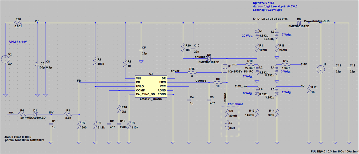
I implemented a flyback converter solution with the lm3481 and have it already running. Due to new design changes I took a deeper look into the simulation which I did in ltspice.

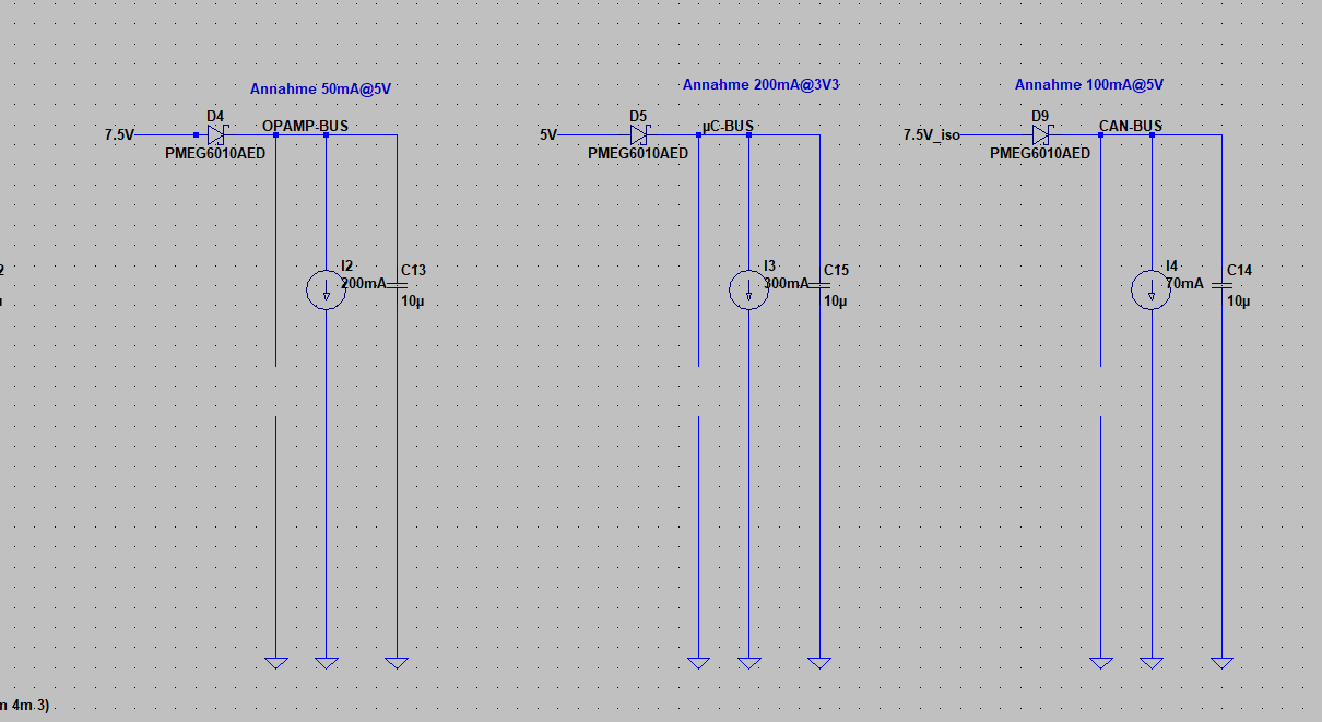
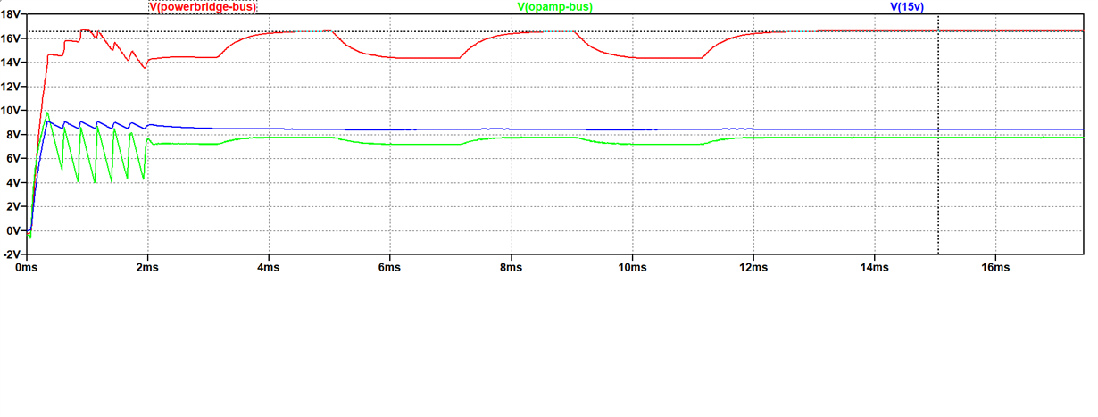
Now when I have a change in loadpower(at 1ms, 5ms, 9ms etc...), in this case on my powerbridge rail I see the output voltages drop. Why don't they start to rise again?

I tried to reduce the feedback voltage divider which reduces the total drop, but still it won't rise. When I reduced the primary inductance L1 to ~1µH it started rising slowly.

Why is that and how can I change it without further reducing L1?

Best regards

Norbert

  • You circuit may not have good cross regulation because the aux rail (+15V) is very light load, making it D1 a peak detector circuit and the rest of the winding most time lose coupling to this regulated rail. To prove this, can you use your max power rail as the feedback rail?
  • Hi Norbert,

    Just another comment, the current sense filter corner frequency is really low (~33kHz) This is well below the switching frequency when it should really be about 10x higher than the switching frequency. This filter is used to just get rid of high frequency noise.

    As Youhao suggests this looks like a cross regulation issue.

    -Garrett
  •   I tried switching the feedback rail to be the max power rail, and also used Garrett's point to change the ISEN filter to ~3MHz. But this makes the circuit even more susceptible  to loadchanges as you can see in the figures.

    I also tried this: http://www.ti.com/lit/an/snva562/snva562.pdf but it doesn't really help.

    When I just add a 70mA load to the feedback circuit (where it says "15V") from my first post, all the other rails rise highly above their nominal voltage. That underlines a cross regulation issue. But how can I resolve such an issue? From my point of view, one always has problems, if there is a significant change in the output load demands.

  • Hello,

    I would appriciate any further help, since im not that familiar with the physics yet.

    Regards

    Norbert

  • Hi Norbert,

    I looks like the compensation network was not updated to meet the new output voltage and load requirements. Please try this since you are not using the 15V rail for the feedback loop anymore.

    In the original configuration please load the 15V rail and use it for the feedback reference. If the rail that is being used for feedback regulation is in a light loading condition and the other rails are heavily loaded the transient response will model likely be poor on the other rails. This is what we mean by cross regulation.

    -Garrett
  •  Hi Garrett,

    thanks for the hint. Im not sure how to match the compensation network to the load requirements. I deleted C2 and C16 to see the impact and the output voltage looks pretty nice. Now, since this will result in a really bad switching behaviour, how can I calculate a good value for the compensation? 

    I tried to get help from this document: http://www.ti.com/lit/an/snva761/snva761.pdf

    But it uses another circuit and I can't find any help in a the datasheet for my case.

    Regards

    Norbert

  • Also, can you explain how the output voltage control works? If it is a current mode controle, how does Vfb influence this? I looked into the functional block diagram and all the explaination given in the lm3481 and lm3478 datasheets, but I still can't get it straight. 

    If every duty cycle is determined by the time when the measured current (Vcs) equals the compensation slope curve (+ the fb-comparator, which is a binary signal if not filtered by a comp network), how can Vfb still have an influence on the output voltage in the case of no compensation network? (as I simulated)

    If a compensation ist added, the function is pretty clear to me (at least if the output is more or less a dc-signal). The fb-comparator output signal reduces the slope compensation just by a small amount if Vfb is higher then its reference, therefore the duty will be decreased and the output voltage drops again, right?

    But that can't be the only use of the compensation network(i.e. to flatten the comparator output), so what's the deal here? In the datasheets and application notes, the compensation network is just applied for boost and/or sepic topologies by calculating the whole transfer function and its zeros and poles. Is there a diffrerent, more applicable way?

    Kind regards

    Norbert