This thread has been locked.

If you have a related question, please click the "Ask a related question" button in the top right corner. The newly created question will be automatically linked to this question.

TPS54540: Compensator check

Part Number: TPS54540

Hi Sir,

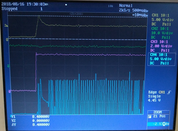
Would you help check the compensator? is it appropriate for switching frequency 950KHz and 650KHz?


Vin=9V to16V, Vout=5V, Iout=3.5A, Maximum ambient temperature=85C, switching frequency= 950KHz and 650KHz

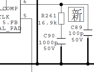
Inductor= 10uH, Output capacitor: 470uF electrolytic capacitor//10uF MLCC

Thanks!

Vito

  • Vito,

    That looks good. I ran the sim in WEBENCH and got a phase margin around 97% at 13kHz so it will be good to react, a bit slow to correct, but it should be stable.

    Here's a link to my WEBENCH design based on your inputs. You can use the, "Re-Comp" tab if you'd like to change your phase margin and crossover freq.

    -Sam

  • Hi Samuel,

    Thank you for your support.

    We set the frequency to 950KHz and observed a voltage spike during start-up. The output voltage go up to around 8V. Could you teach me how to solve this issue?

  • Vito,

    This should only happen if the converter is switching for too long - VOUT is regulated but it keeps switching for some reason. Possible reasons:

    1. FB is low when it shouldn't be (could be due to layout).
    2. COMP values are incorrect (but they look okay).
    3. The IC is unstable (comp values or layout).

    Please share the layout and I'll take a look.

    -Sam
  • Hi Samuel,

    Our customer told me that they did not see the voltage spike when the TPS54540 operated at 650KHz. I will try to get layout file.

    BTW, can you re-check the compensator? We need them operate at both 950KHz and 650KHz.

    Thanks!

    Vito

  • Hi Samuel,

    Enclosed please kindly find the layout file.

    I have a question. The TPS54540 has built-in an output overvoltage protection. Why was the OVP not triggered?

    MAIN-P4C1249ZA-PP0-PCB-180717_DCDC.pdf

    Thanks!

    Vito

  • Vito,

    Switching frequency is not tightly linked with stability so you should not have to recompensate for a different switching frequency. The only time that would be the case is if the lower frequency bandwidth was wide enough to interfere with the crossover freq but you're seeing issues at a higher frequency which leads me to believe compensation is not the issue.

    OVP would trip if FB (with respect to the GND pin) was >106% ref. Clearly FB is above 106% and it looks like it's still switching (for a millisecond or two). This leads me to believe there's an issue with the GND part of the FB to GND measurement.

    You will have to check the IC's operation as this issue occurs. Use a scope to see what's happening on the pins. Is FB noisy? Is VIN noisy? How does this all compare to the 650kHz board? Here are some thoughts of things to try from what I saw in the layout:

    Your attached layout shows the GND pin is not connected to the thermal pad or to a large GND plane. Instead it goes straight to a via to a plane in the mid-layer. That means all return (GND) current must go through mid/bottom layers and through that via to get to the GND pin of the IC. All this parasitic inductance may be resonating at a harmonic of 950kHz (but not 650kHz) which could cause a GND bounce issue. This would explain what you're seeing. You can try some careful soldering to connect the GND pin pad to the thermal pad under the IC to confirm if this would help fix the issue.

    The VIN caps should also have a shorter loop. C77 is close to VIN (good) but it goes through C78 which will require a long path and multiple vias to get back to the GND pin of the IC. This should be a very small loop. You can try connecting a wire directly from C78 GND pin to the GND pin of the IC to see if this helps.

    Other layout guidelines are in the datasheet.

    -Sam
  • Hi Samuel,

    Thank you for your prompt reply. We will try to improve ground connection.

    Thanks!
    Vito
  • Hi Samuel,

    We connected the GND pin pad to the thermal pad under the IC and connected C78 GND pin to the GND pin of the IC. But it doesn't work. The issue cannot be solved.

    Yellow: VOUT

    Green: VIN

    Red: EN

    Blue: SW

    Thanks!

    Vito

  • Vito,

    Your scope capture shows the spike only occurs on the first startup and I'm not sure if that's because of the resolution of the picture. Please clarify.

    Can you send another picture showing those same 4 waveforms but zoom in so the screen starts when EN goes high and ends when VOUT has settled? I'd like to see the SW behavior during this issue.

    You will have to check the IC's operation as this issue occurs. Use a scope to see what's happening on the pins. Is FB noisy? Is VIN noisy? How does this all compare to the 650kHz board?

    -Sam
  • Hi Samuel,

    The issue only occurs on first startup. You can see the vin rises from 0V to 12V.  We don't see the spike if we disable the IC and then enable the IC ( the power supply is kept ON).

    Thanks!

    Vito

  • Vito,

    I see from your first picture that VIN comes up and everything spikes a bit. Then EN is enabled and we see the spike on VOUT when VIN was already on.

    -Sam
  • Hi Samuel,

    Please ignore my previous post. The issue occurs when the IC is enabled.

    Please refer to attached pictures.

    Thanks!

    VitoTPS54540 measurement 20180817.xlsx

  • Hi Samuel,

    Please take a look at the measured waveforms and teach us how to solve this issue.

    Thanks!
    Vito
  • Vito,

    My leading theory is that the 950kHz (or the harmonics of 950kHz) is ringing with some parasitic caused by the layout. The GND pin is connected to the rest of the board through a small trace and a single via. It should be connected directly to the thermal pad on a large top layer GND pour and I think this might be where the issue is coming from.

    From your waveforms FB is greater than 106% regulation and the part is still switching. This probably means the way FB is measured in your waveforms is not the way the IC is measuring FB. Make sure you're measuring FB with respect to the GND pin on the IC. Try to solder a twisted pair as close as possible, or on the pins of the IC to make sure. Check the waveform of FB with respect to the GND pin of the IC on a scope. Zoom in to see a few switch cycles during this issue to make sure the IC is seeing >106% Vref on FB.

    -Sam
  • Hi Samuel,

    The way I measured FB is similar to attached file.

    Thanks!

    Vito

  • Vito,

    To clarify, the scope captures you attached before were taken with FB probed like this?:

    -Sam

  • Hi Samuel,

    Yes, you are correct.

    Thanks!
    Vito
  • Hi Samuel,

    Yes,  the fb was probed similar to the picture you attached.

    Vito

  • Hi Vito,

    Sorry for my delayed reply. I am having another engineer look at this with me.

    -Sam
  • Hi Samuel,

    We did a cross-reference between TPS54540-Q1 EVM and customer’s board. We installed customer’s TPS54540, inductor (L10), output capacitor (C86, C87), diode (D16) onto EVM, set EVM frequency to 950KHz and used the same comp values. We connected the EVM to customer’s board and confirmed there is no spike.

    We want to reproduce the issue using EVM. We cut the connection between IC GND pin and the thermal pad under the IC for the EVM. We connected the EVM to customer’s board and confirmed there is no spike.

    Do you have any suggestions on PCB layout improvement or component change?

    Thanks!

    Vito

  • Hi Samuel,

    The issue is not solved. Please help on this.

    Thanks!
    Vito
  • Vito,

    This is a difficult issue. It is not straightforward what the issue is but we can do work to try to nail it down.

    1. Can you try depopulating R257 and set R256 to give you 950kHz. The capacitance or something to do with Q14 may be messing with this sensitive node.

    2. What happens to the spike behavior if you try different frequencies? Try 700kHz, 800kHz... does the spike get worse as the frequency increases? Or does it click on at a certain frequency.

    3. Please confirm that the spike happens at every power-on, not just the first one like I saw from the picture.

    -Sam
  • Hi Samuel,

    The spike happens at every power-on. I will try 1 and 2.

    Thanks!
    Vito
  • Hi Samuel,

    The spike got higher when we increased the fsw. 

    We observed that the output voltage keeps going up after soft-start time and starts falling down after 2ms.

    All the measurement are done with the same board. The IC GND pin is connected to the thermal pad under the IC.

    BTW, we have added a 470uF capacitor very close to IC VIN pin and GND pin. But the issue did not go away.

    Thanks!

    Vito

    TPS54540 measurement 20180824.xlsx

  • Vito,

    It looks like 850kHz is has a very similar overshoot to 950kHz but 650kHz has no overshoot at all. Just a small spike that looks like the start of an overshoot. Did you test 700kHz, 750kHz, or 800kHz? It would be useful to see this trend.

    Let me get another engineer involved. In the meantime:

    • Try placing a 1uF ceramic cap between L10 and C86 connecting from VOUT to GND. Give a short clear path to the GND pin of the IC.
    • Rotate C89 (CCOMP) so that the GND pad is connected to the GND plane below the Cboot trace. The current path to GND may be corrupted as compared to the other CCOMP. Or rotate C90 to connect the GND pad to the GND pad of C89. I'd just like them both to have the same GND connection.

    -Sam

  • Vito,

    I've been talking with an engineer Robert Blattner about this. He knows more about this part so he will take over the analysis from here. I'll still be monitoring but he will be the engineer on this thread.

    Quick question - What's the part number on the diode?

    -Sam
  • Hello Vito,

    In the past, we have seen poor behavior during soft start if the SW is noisy and frequency is high. There may also be lot to lot variation in this behavior. I recommend the following steps for continued debug:

    1) Forward the diode’s part number so we can check its specifications.
    2) Get a close up showing the SW during soft start, we are looking for overshoot, under shoot, and ringing during each switch cycle. One or a few switch cycles should be good enough.
    3) Try one of the customer’s TPS54540s in your EVM.
    4) Try a TPS54540B-Q1 in the customer’s board and see if the overshoot goes away. This part is beefed up to be more resistant to this kind of noise.

    Regards, Robert
  • Hi Robert, Samuel,

    Thank you for your support.

    1) Forward the diode’s part number so we can check its specifications.
    May I know what is your concern about the diode?

    3) Try one of the customer’s TPS54540s in your EVM.
    Please see me post on Aug 22, 2018 10:22AM, We installed customer’s TPS54540, inductor (L10), output capacitor (C86, C87), diode (D16) onto EVM. We did not see the spike.

    I will try 2 and 4 on Monday.

    Thanks!
    Vito
  • Hi Robert, Samuel,

    1. We placed a 1uF ceramic cap between L10 and C86 and moved C90 to very close to C89. Unfortunately, the spike is still present.

    2. We installed EVM's diode PDS760-13 onto customer's board. We confirmed that the spike disappear.

    3. Customer's diode part number is B540C-13-F.

    ds13012.pdf

    4. Enclosed please kindly find the SW waveform measurement.

    TPS54540 measurement 20180827.xlsx

    BTW, we are requested to solve this issue by this Wednesday. Please help on this.

    Thanks!

    Vito

  • Hello Vito,

    The large input loop – see figure below – combined with the parasitic inductance of the diode is causing a noisy switching waveform. This can be seen by undershoot when the switch node falls in the waveforms that you provided.  Even with the EVM diode, this voltage reaches -5 V. 


    In higher frequency circuits, the chip is exposed to more noise making it more sensitive. There are four things you can do to fix this:

    1. Most recommended: Use the TPS54540B-Q1 family. We beefed up internal circuitry so that this device can withstand more switching noise.

    2. Reduce the input loop: If it is difficult to move the large input capacitors, add a second pair of smaller caps. 100 nF will due for a second pair. See figure below for proposed location.

    3. Choose a lower inductance diode like the one in the EVM or add a second diode in parallel.

    4. Try a SW node snubber: 5R0 in series with 100 pF should work well. The ground side of the snubber should be as close to the chip’s ground, DAP is OK, as possible.


    Since this design is marginal, I recommend running up frequency to see how much margin the final design has and to compare solutions. Having a max frequency rather than pass / fail will allow alternative solutions to be compared.  Using the TPS54540B-Q1 will increase maximum frequency more than the other solutions recommended so will require less redesign.

    Regards, Robert

  • Hi Robert,

    The switching waveforms I provided yesterday which were done with customer’s diode B540C-13-F, not EVM diode PDS760-13.


    I cannot find inductance information from PDS760-13 datasheet and B540C datasheet. Can you please teach me where I can find the inductance information and how to select the diode?


    With another diode B540C-13-F in parallel with D16 and set Fsw to 950KHz:

    1. We confirmed that there is no spike during startup. Please refer to Figure 1 and Figure 2.
    2. Figure 3, during soft-start time, the voltage reaches over -4V.
    3. Figure 4, at steady-state, we don’t see negative voltage.


    With another diode B540C-13-F in parallel with D16 and set Fsw to 1.2MHz, we can see spike during start-up. Please refer to Figure 5.

    With another diode B540C-13-F in parallel with D16 and set Fsw to 1.5MHz, we can see spike during start-up. Please refer to Figure 8.


    We set fsw to 1.2MHz, added a 1uF capacitor close to chip, added a SW node snubber and a B540 in parallel with D16 . The spike is still present.


    TPS54540 measurement 20180828.xlsx

    Here is the summary of the test result. 

    FSW 950KHz 1.2MHz 1.5MHz
    another B540 in parallel no spike spike spike
    another B540 in parallel + 1uF VIN cap.   spike  
    another B540 in parallel + 1uF VIN cap. + RC snubber   spike  

    Would you explain the reason why diode inductance/switch noise cause the output spike at power-on?

    Best regards,

    Vito

  • Hello Vito,

    Thank you for performing the experiments that we suggested.

    Unfortunately, many diode manufactures to not share their inductance values in their datasheets. Often, this information is listed in their detailed package information which is usually separate from the diode’s datasheet since many diodes share the same package.  If this information is not available on the web, sometimes the diode manufacturer will share this information if contacted.

    The reason that switch node pulses have negative spikes during startup is that the load current is heavier during startup. During startup, the output capacitors are charged in addition to any load present.  With the output cap that you have, this is between 1.2 A to 1.6 A extra during startup.  Any capacitance in the load will add to this current.  Note that during this period, the native spikes, while better with two diodes is still exceeding the part’s ABS MAX specification. 

    It looks like you have a solution with two diodes but do not have good margin. The 1.2 MHz check shows that this design is still marginal.  The best solution is to use the TPS54540B-Q1.  The reason that a noisy and high frequency switch node can cause the overshoot is twofold:  The first reason is that in this IC, ground is designed to be the lowest potential with only PN junctions and substrate resistance to isolate analog circuitry.  The second reason is that with only junctions to isolate devices, noise can more easily get into analog circuitry than if devices were isolated with insulators such as in a discrete solution on a PCB.  Since junctions conduct when forward biased, the IC is most sensitive to switch noise while switch is below ground.  In order to overcome noise, in the TPS54540B-Q1 we beefed up (increase current drive capability of) analog circuitry allowing this device to tolerate more noise.

    Regards, Robert

  • Hi Robert,

    Thank you for the explanation.

    Customer will ask their diode vendor to provide more detailed information. Can you please specify/list what parameters we need to consider for high frequency application?

    Thanks!

    Vito

  • Hello Vito,

    Before discussing the diode, please see if you can switch your customer the B-Q1 version of this IC, doing so will get more margin in the design than selecting a better diode. It will also eliminate a variable, the diode, from design analysis. We have improved internal circuitry in the version to making the IC more tolerant of a noisy SW node. Please use the TPS54540B-Q1 rather than the TPS54540. Please contact me directly if there is a reason that should not be on a public forum preventing the customer from adopting the TPS54540B-Q1.

    As for the Schottky diode, there are three factors:

    1) Inductance: high inductance slows down the rate at which the diode can turn on. This causes undershoot.

    2) Capacitance: While the SW node is falling, a portion of the inductor’s current is provided by the diode due to the diode’s capacitance. This current reduces undershoot. Chose a Schottky with similar capacitance to the EVM’s diode. Note that too much capacitance will cause excessive ringing during turn on of the IC’s high side FET so do not exceed the EVM’s diode’s capacitance by more than a factor of 3.

    3) Forward drop: low forward drop < 0.5 V while conducting peak current is desirable. This effects the switching waveform in two ways:

    a. Below 0.5 V, there is none of the junction diode effect called conductivity modulation. If forward drop during DC conduction is > 0.5 V, the diode’s resistance includes this effect. Since this effect turns on slowly, the diode will have a higher forward drop than expected during the first few nanoseconds of conduction. This can increase undershoot on the switch node.

    b. A low forward drop decreases the negative voltage in general during conduction, reducing undershoot.

    Regards, Robert
  • Hi Robert,

    Thank you for your great support.
    Vito