This thread has been locked.

If you have a related question, please click the "Ask a related question" button in the top right corner. The newly created question will be automatically linked to this question.

LM3481: The flyback circuit for LM3481

Part Number: LM3481
Other Parts Discussed in Thread: TL431

Hi, 

       I am trying to design flyback dc-dc converter using LM3481. I have used the calculator software from Ti for LM3481 and simulated the circuit in ltspice for input 19V to 36V the output 24V.

  This is working very good in ltspice and for confirmation I have also simulated 12V output circuit in ltspice with values obtained in calculator software. 

Please see the circuit and simulation for 24V below

Can you please check this and let me know if there is a mistake? 

Also, I am not sure that it is correct to attach 4.7K between Comp and VCC pins, I have just replicate it from LM3481 EVM?

Thank you.

Kind regards

Mohsin

  • Hi Mohsin,

    Please flow the guide that describes how to design the LM3481 as a flyback. I would double check and see if the voltage reference and the resistor values are setting the output voltage correctly. This is a common mistake as some references are 1.25V and some are 2.5V.

    The 4.7kOhm resistor is common and is just used as a pull up resistor. 

    -Garrett

  • Hi Garrett

    Thank you for your quick reply.

    The voltage reference for TL431 is 2.5V and I have done calculations with respect to 2.5V.

    I have developed this circuit on vero board and tested.

    I am observing continuous increasing output voltage. It means that may be the feedback circuit is not working properly.
    Also, when I put a 1k ohm resistor on the output, it burns out after some time.
  • Mohsin,

    Please try following the compensation approach that is suggested in the application note.

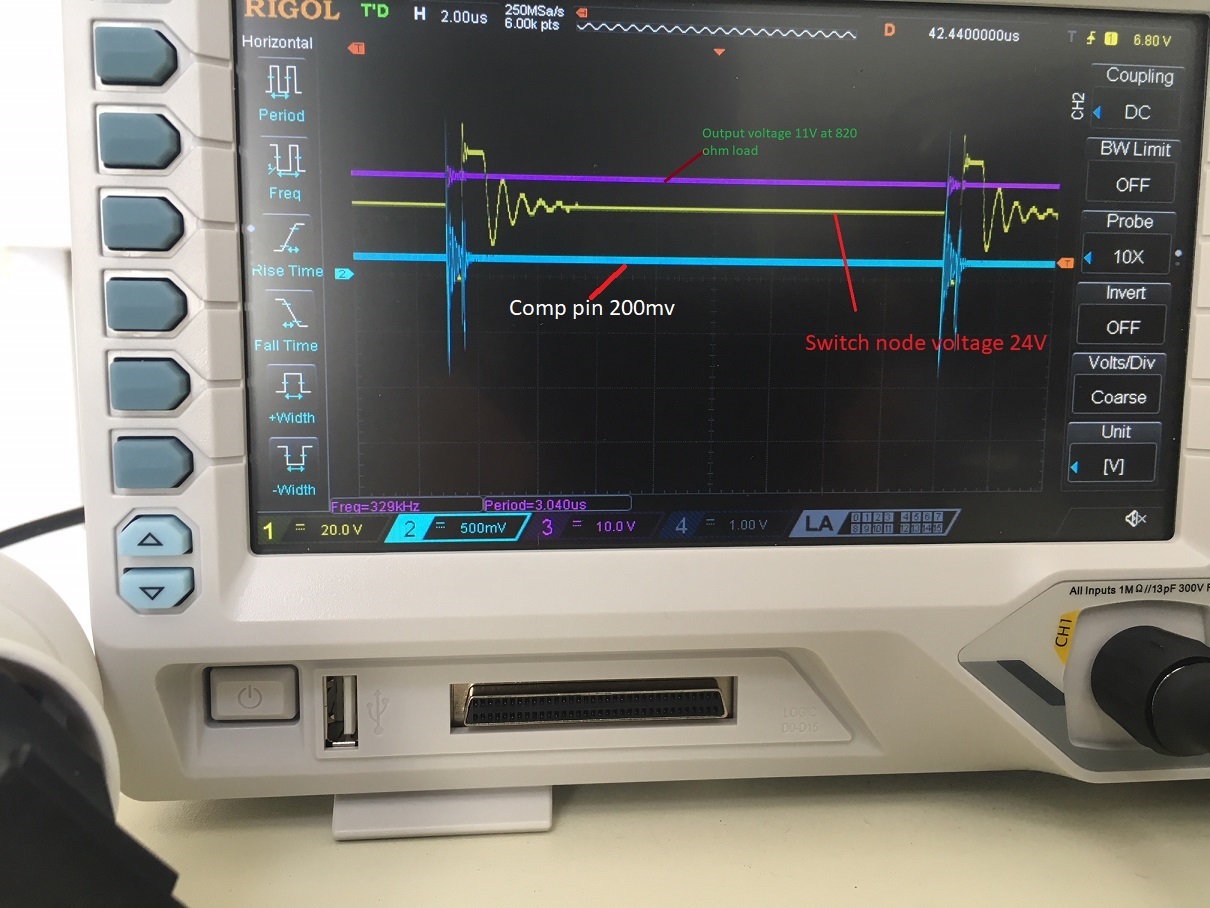
    Can you post a picture of the output voltage rise, COMP and the switch node voltage on the same scope plot? This will help to debug the issue.

    Thanks,

    Garrett
  • Hi Garrett,

         Thank you.

           I have tried to follow the application note provided and have developed a new circuit for 11V output.

    From application note, I could not understand that how 3KHz cross frequency was selected and how 400 Hz is selected as zero for compensation. Also it is difficult to produce the Bode plot for my design. So I just calculated the using same bode plot and selected zero at 800Hz. Can you please refer me some other document for it?

    Now, please find below the circuit with simulation results and Oscilloscope scope capture of the vero-board implementation. 

    I have set the switching frequency to 416 KHz. The Oscilloscope results of bench shows that the IC is not generating the switching frequency of 416 KHz.

    Can you please help me to debug this that where I am making a mistake?


    Thank you.

    Kind regards

    Mohsin