


Hi:
I originally posted this message in the Sitara Processors Forum. The following is a copy of the dialog between myself and a TI employee who ultimately suggested I post it here also...
---------------------
Hi:
I have a new design using the above components. I am using a 25 MHz clock osc to clock OSC0.
I find that I have a signal on the power rail outputs of the 65217, particularly on L2 and L3 (VDD_MPU and VDD_CORE) The signal is roughly sinusoidal and varies somewhat in frequency between 27 kHz and 30 kHz. The signal varies in amplitude, board to board, from almost nothing to maybe 400 mVpp worst case. It also appears that L1 (VDD_DDR) is also affected but not as severely as L2 and L3. Of these 2, L3 is more severely affected than L2. The LDO outputs of the 65217 are clean. I also have 5v and 3.3v supplies on the board which power everything else (including the 65217) and they are also clean as are my grounds.
This bothersome signal is present even when not running code (i.e the 3354 is not allowed to boot) and all other oscillators on the board are disabled. The signal disappears when I kill the 25 MHz clock osc. so the 65217 and associated filtering are generating clean voltages. I followed all grounding recommendations in the AM335x datasheet when using an LVCMOS clock oscillator for OSC0 and my routing doesn't appear to be a factor.
Anyone have any experience with this?
Thanks
----------------------------
What power rail is powering the oscillator and what is the oscillator output voltage?
Regards,
Paul
--------------------------
Hi Paul!
It's an LVCMOS osc powered from LS2_OUT of the 65217 (VPP_3P3) and is 3.3v pp (With a tad of overshoot about 3.5vpp) VDD_3P3 looks clean.
--------------------------
The OSC0 input should not be connected to a 3.3 volt clock source.
The data sheet shows the oscillator connected to OSC0 powered by the VDDS_OSC power rail which should be 1.8 volts.
Regards,
Paul
---------------------
I modified 2 boards to use a 1.8v clock osc. with no improvement. I should add that I am already powering the VDD_OSC power domain at 1.8v and powering the 1.8v clock osc from the same source.
--------------------------
In your first post, you mentioned this was observed even when you did not allow the AM335x device to boot. What did you do to prevent it from booting? The ROM code would still be running if you were not holding PWRONRSTn low. What happens if PWRONRSTn is held low?
Could this be ripple on the switching power supply outputs that is only observed once the master clock reference is applied and the processor begins to draw current?
I haven't seen many customers use a LVCMOS oscillator as the reference clock source. To eliminate any unexpected interaction with the LVCMOS oscillator, how hard would it be to modify one these boards to remove the oscillator and connect a crystal circuit?
Regards,
Paul
-----------------------------
>>In your first post, you mentioned this was observed even when you did not allow the AM335x device to boot. What did you do to prevent it from booting? The ROM code would still be running if you were not holding PWRONRSTn low. What happens if PWRONRSTn is held low?<<
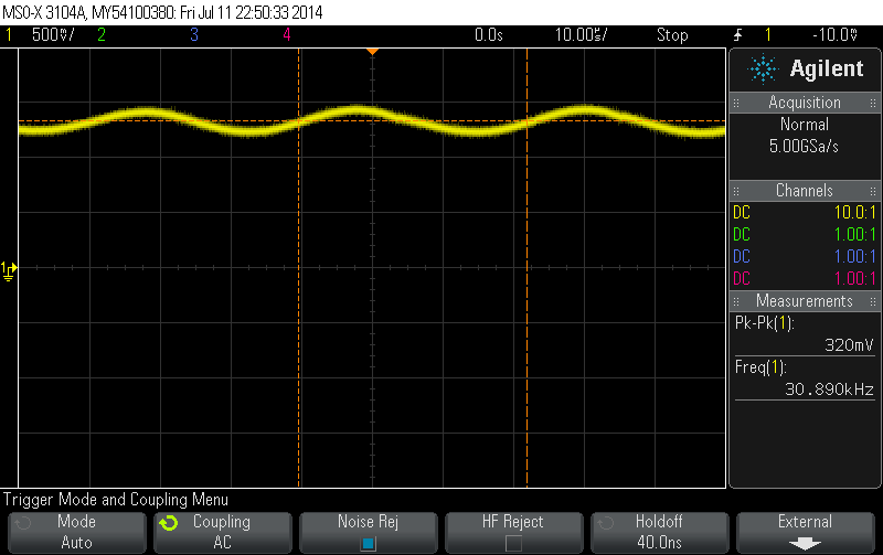
We are booting from an SD card and I was only disabling that. You are correct in that ROM was still executing. When I hold PORZ low the signal on the rails drops dramatically. It doesn't go away completely but, on the board I have, it drops to about 100 mVpp vs. 350 mVpp. That is measured with the 25 MHz oscillator still running. So perhaps this signal is power supply ripple that only becomes apparent when the processor start to pull significant current. Keep in mind that the signal I'm seeing is around 28 MHz and the switching frequency of the 65217 is around 2.25 mHz.
Unfortunately, I cannot modify a board to use a crystal circuit. I am revving the board however to make some other changes and I will certainly use the recommended crystal circuit in place of the oscillator.
------------------------
Your first post said the power supply noise was 27 - 30 KHz, but your last post said it was 28 MHz.
You may want to post your observations on the E2E forum that supports the PMIC to see if they have any suggestions.
I would like to provide an additional comment related to using a crystal circuit vs LVCMOS oscillator. I do not know any reason you should not use a 1.8 volt LVCMOS oscillator. We just do not see them used very often because customers prefer to purchase the lower cost option which is the crystal. I think you would be seeing the same power supply noise if you were using a crystal circuit rather than the LVCMOS oscillator. Using an LVCMOS oscillator could improve noise immunity of your product if it is going to be exposed to a environment with lots of electrical noise. There have been cases where noise has coupled into the crystal circuit which cause it to be injected on the slow changing sinusoidal signal generated by the crystal circuit and this noise was large enough to generate glitches on the internal clock signal as the noisy sinusoidal signal transitions through the switching threshold of the input buffer. See Advisory 1.0.30 in the AM335x Silicon Errata for more details.
Regards,
Paul
