This thread has been locked.

If you have a related question, please click the "Ask a related question" button in the top right corner. The newly created question will be automatically linked to this question.

PWM settings of Vibrator driver of TPS65930

Other Parts Discussed in Thread: TPS65930

Hi All,

We are trying to control the output voltage of the VIBRA_P/VIBRA_N of the TPS65930 vibrator section through VIBRA_SET[7:0] register. I have a couple of questions.

1. The minimum differential output swing as specified in the Vibrator H-Bridge section of the TPS65930 datasheet is 3.6V, though the VBAT is only 2.8V.  How does  the TPS65930 achieve this? Please clarify,

2. Currently, we are using a vibrator which can operate till 3.6V. As the existing vibrator is obsolete, we are forced to use a vibrator(Z3OC1T8219731) which can operate till 3.2V(We had to match the mechanical dimension as well. Hence the limitation). We are trying to change the Vibrator differential output voltage to match that of the vibrator. Changing the values of the VIBRA_SET[7:0] register is having no effect on the vibrator output voltage. The value of the VIBRA_CTL register is 0x01. 

Please let us know if we are missing anything to make the VIBRA_SET[7:0] register changes to take effect.

Thanks & Regards,

Naveen

  • Eagerly awaiting a reply...
  • Any suggestions would be greatly appreciated.

  • Hi Naveen,

    Sorry for the delay, yesterday was a holiday in the U.S.

    1. The VPP is measured across the VIBRA.P / VIBRA.N connections. It generates a positive voltage when operating one way (current from P to N) and negative voltage when operating the other way (current from N to P), creating a differential. Note this differential cannot exceed 2xVin.

    2. I see the Minimum differential output swing appears to be 3.6V, are you saying you need 3.2V instead? And that the VPP is the same from VIBRA_SET = 0xFF vs. VIBRA_SET = 0x01? If so, can you post scope shots of both differential (VIBRA.P relative to VIBRA.N) and single ended (VIBRA.P relative to GND and VIBRA.N relative to GND) for both VIBRA_SET conditions? This will allows us to ensure that the circuit isn't bottoming out.
  • Hi Kevin,

    Thanks for the detailed reply.

    Yes, we need 3.2V instead of the default minimum 3.6V and we are not seeing the change in VPP for VIBRA_SET = 0xFF vs. VIBRA_SET = 0x01.

    Here are the snapshots of the vibrator pins:

    VIBRA_P_VIBRA_SET = 0xFF

    VIBRA_N_VIBRA_SET = 0xFF

    DIFF_VIBRA_SET = 0xFF

    VIBRA_P_VIBRA_SET = 0x01

    VIBRA_N_VIBRA_SET = 0x01

    DIFF_VIBRA_SET = 0x01

    Register settings are as follows:

    VIBRA_CTL(Address Offset 0x45) = 0x01

    CODEC_MODE(Address Offset 0x01) = 0x02

    VIBRA_SET(Address Offset 0x46) = 0xFF and 0x01

    Please let us know if we are missing anything here.

    Thanks & Regards,

    Naveen

  • Hi Naveen,

    What Vin are you using? Note that due to it being a simple driver in this configuration, the Vin will always pass to the Vout when the high side is on; we are just modulating the voltage to get a set current value. If you need a lower voltage, you could potentially try a resistor in series if you know your current?

    That said, I would expect the VIBRAP to be oscillating with the internal PWM signal. VIBRAN should be short to GND with your configuration.

    What value do you have in the VIBRATOR_CFG register? If VIB_PWM = 0, then that might explain why there is no PWM. Also, PMBR1 needs to be set so that GPIO7 is in the appropriate mode (as GPIO7 or as VIBRASYNC if you are using VIBRASYNC). Also, LEDA and LEDB need to be disabled.
  • Hi Kevin,

    Vin voltage is 3.8V in our design. Thanks for suggesting external resistor option. We will explore the same.

    We are not grounding VIBRA_N pin in our design. Can you please elaborate on why it should be grounded?

    Regarding VIBRATOR_CFG register, it was initially set to 0x00. And we are not using VIBRASYNC option in our design.

    We are not able to understand the address offset specified in the VIBRATOR_CFG register. It is mentioned as 0x05-0x05 in 0x17 bytes increments. How do we interpret this address offset?

    We have another query on the PWM control. How are the duty cycle settings in VIB_DSEL and VIBRA_SET[7:0] registers related? Do we need to use only one of them?

    Your suggestions would be greatly helpful.

    Thanks & Regards,

    Naveen

  • Hi Naveen,

    There is no need to GND VIBRA.N, it should be shorted to GND internally since the VIBRA_SEL = 0 and VIBRA_DIR = 0 --> Driver M = 0 (Figure 10-1 in TRM). 

    For the I2C, I believe you can ignore the physical address and increment and just focus on the 0x05 = register address. Looking VIBRATOR_CFG up in the I2C address tables (Table 2-6) shows it listed under device I2C address 0x4B. Those two should be enough to bit bang that particular register, let me know if it works or not.

    Regarding VIB_DSEL and VIBRA_SET, I believe they operate on two different scales. The VIBRA_SET sets a PWM frequency of the drivers (short time scale, us or ms range) with the intent that the low pass filter that is the DC motor will cause a reduced overall voltage / current / intensity. The VIB_DSEL appears to work in the 100s of ms scale by enabling / disabling the whole vibrator block. If you want the vibrator to pulse, you can use the VIB_DSEL to do this, otherwise it can just be left at 00.

  • Hi Kevin,

    We are still not observing the PWM output even after setting the VIBRATOR_CFG register to 0x04( Even tried other values for PWM changes) with 0x05 = register address. 

    The voltage output we are observing is around 3.7V at VIBRA_P even when Vin is around 3.9V. Is it normal?

    Thanks,

    Naveen

  • Hi Naveen,

    What do you have attached to the VIBRA_P? The 3.9V -> 3.7V drop could be the IR drop due to the driver and would depend on your load, the main issue appears to still be the lack of PWM. 

    To confirm, does toggling CODECPDZ in CODEC_MODE register or the CLK256FS_EN bit in the AUDIO_IF register have any effect on your system? 

  • Hi Kevin,

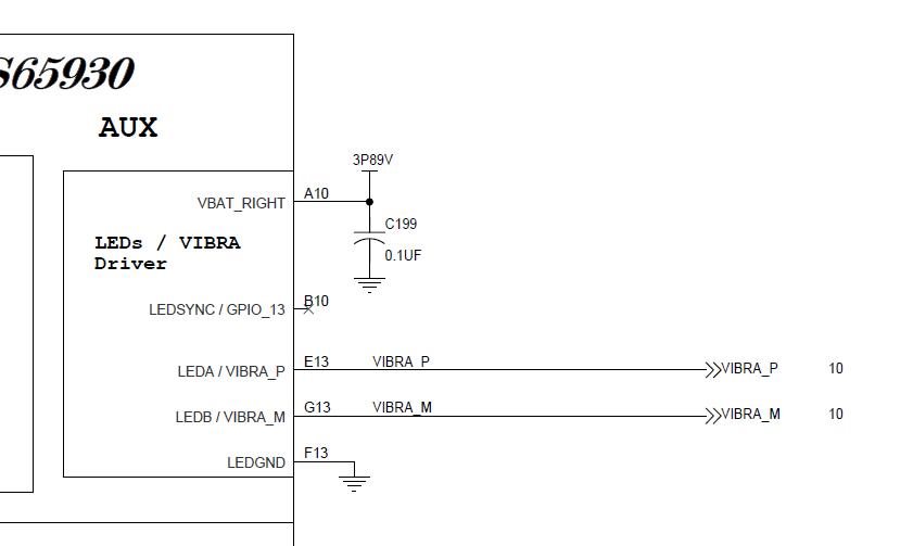
    The vibrator connection in our design is as shown in the image below:

    Before trying the other register options, I would like to confirm with you if there is a sequence in which all the registers associated with Vibrator are to be set.

    We are setting the registers through I2CSET commands in no particular order. Please suggest.

    Thanks,

    Naveen

  • Hi Naveen,

    The order should be same as 10.5.1 Vibrator H-Bridge in the TRM, though of course modified to your application:

    1. Disable LEDA: Set the LEDEN[0] LEDAON bit to logic 0.
    2. Disable LEDB: Set the LEDEN[1] LEDBON bit to logic 0.
    3. Turn on the codec: Set the CODEC_MODE[1] CODECPDZ bit to 1.
    4. Set VIBRA_SET to desired (0x0F for example)
    5. Set VIBRA_CTL to 0x01

    One additional thing you can check is if setting VIBRA_CTL[1]VIBRA_DIR to 1, do you see the VIBRA_P short to GND and VIBRA_M voltage go to 3.7V? This would allow us to at least confirm that the I2C writes are working as expected.