This thread has been locked.

If you have a related question, please click the "Ask a related question" button in the top right corner. The newly created question will be automatically linked to this question.

TPS650830: VR3 is unexpected turned off while system enter DEEP SLEEP S4/S5 mode

Part Number: TPS650830

Hi,

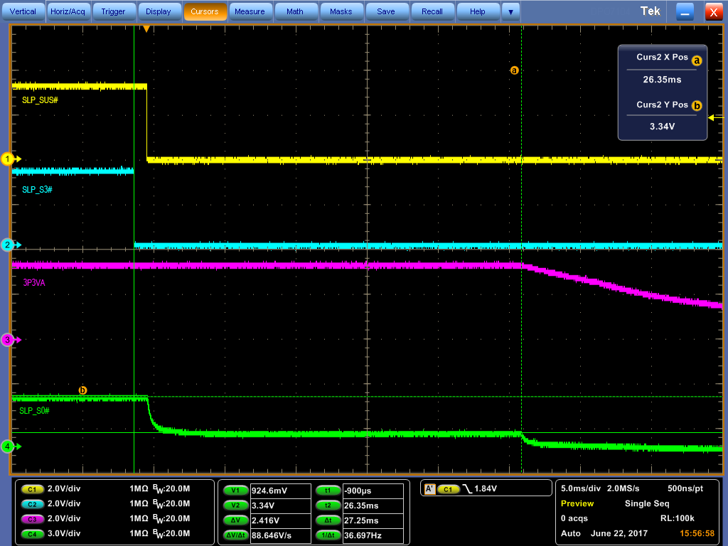
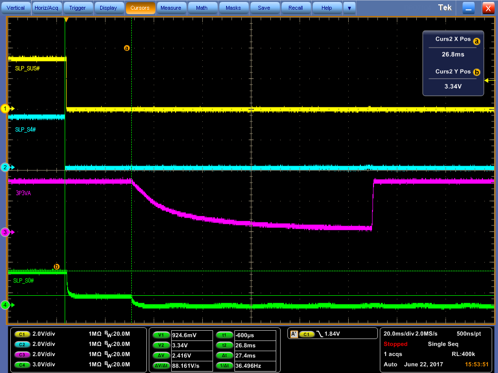
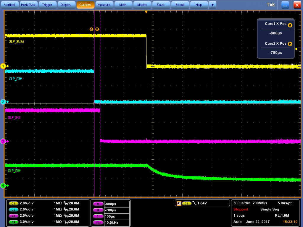
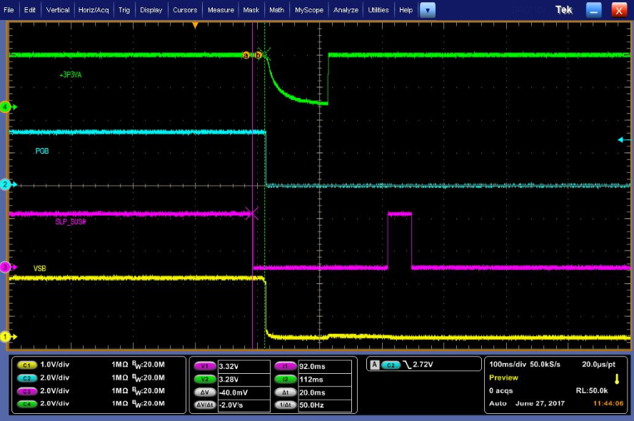
Customer found VR3 is unexpected turned off while system enter DEEP SLEEP S4/S5 mode, and be turned on automatically some time later.  Related waveform w hile it enter sleep mode is as below.  May i have your comments why VR3 is turned off at this moment?

Thanks!

Antony

  • Hi Antony,

    Which signal is 3P3VA: V3P3A_DSW, V3P3A_RTC, or V3P3A_PCH?

    What is ENVR3 connected to?
  • Hi Kevin,

    +3P3VA is VR3 output (V3P3A_DSW).  Additionally, they found 0x16 is read as 0x04 indicating a power fault for V18U_25U.  I also see them providing 2.5V to VSB.  Do we expect 1.8V for VSB?  Should they change VSB to VR2 output which supply 1.8V?

    Thanks!

    Antony

  • Hi Antony,

    VSB is expecting 1.8V; it can either be connected to 1.8V or it cna be connected to a resistor divider from 2.5V:
    e2e.ti.com/.../3202.how-to-connect-pmic-pins-for-ddr3l-lpddr4-lpddr3-etc-memory-types
  • Hi kevin,

    THey try to connect VR2 output (1.8V)to VSB, but the result is still the same as below.

    What else comments do you have?

    Thanks!


    Antony

  • Hi,

    Currently customers  try two ways to provide 1.8V to VSB as below.

    1. Connect VR2 output(1.8V) to VSB directly

    2. Connect VR3 output(3.3V) to VSB through a resistive divider.

    They can still see the original issue with case1 but issue is not seen for case2.  May i have your comments?


    Thanks!


    Antony

  • Antony,

    What is enable signal for VR2? Is it SLP_SUS# or DPWROK signal. There is 32ms delay between VSB and PGB signal, i.e PMIC expects V1.8U_2.5U signal to be enabled for 32ms longer after SLP_S4# signal goes low. It is a good practice to add delay between SLP_S4#, SLP_S3# and SLP_SUS# signal by few tens of ms to avoid any issue.

    Regards,
    Jay
  • Hi Jay,

    They're connecting ENVR2 from SLP_SUS instead of DPWROK. 

    Do you propose them to add >32ms delay from “the falling edge of SLP_S4/SLP_S3” to “the falling edge of SLP_SUS” and connect VR2 output to VSB?

    In our ref design, we connect ENVR2 from DPWROK, and VSB from V1.8U_2.5U which is from VR2/V1.8A enabled by PGB.  By doing so, do we also expect SLPSUS to become low at least 32ms after SLP_S4 is driven low?  Do we specify this in datasheet?

    Thanks!

    Antony

  • Hi Jay,

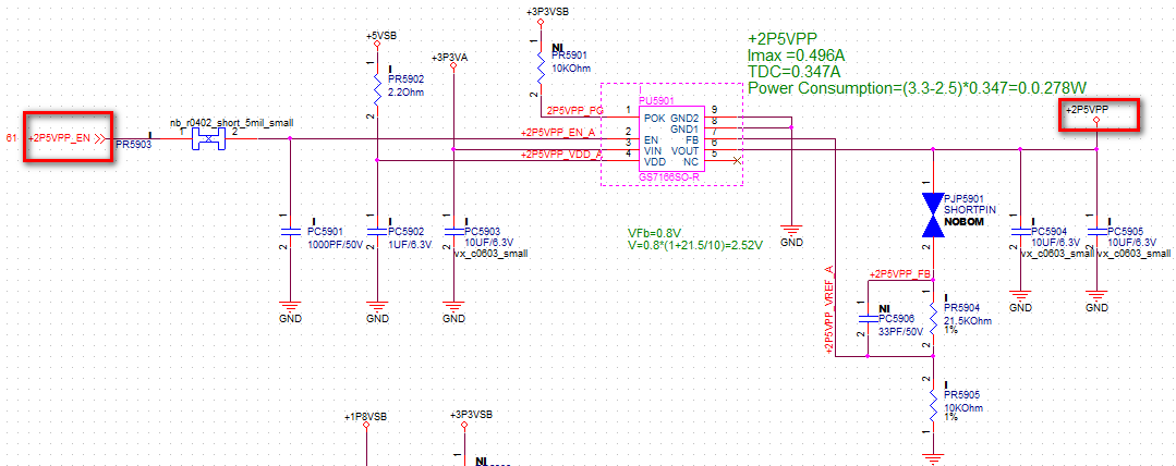
    THe original customer design is described as below.

    • ENB is from SLP_S4
    • VSB is from the 2.5V load switch enabled by PGB (load switch's input is from VR5 output)
    • ENVR2 is from SLP_SUS

    Now they told me the original issue is not seen if either modification as below is made:

    • Case1 : Adding 50ms delay on SLP_SUS
    • Case2: Change the 2.5V load switch input from VR5 output to LDO5V

    Can you explain why the issue not seen in either case as described above?  Besides, i still don't fully understand regarding " There is 32ms delay between VSB and PGB signal" and how it affect this issue.  Can you explain with more details?

    Thanks!

    Antony

  • Antony,

    PGB is enable signal of the load switch 2.5V. If SLP_S4# is disabled, there is PMIC internal delay of 32ms for PGB to go low. If SLP_SUS# is disabled, VR5 rail is disabled.

    In customer case, if SLP_S4# signal and SLP_SUS# signal are disabled together VR5 is disabled but PGB is still high. On the load switch, input (VR5) is disabled and enable signal is high and VSB pin does not sense any input and PMIC goes to emergency shutdown.

    Case1: If delay is added between Sleep signal, this problem is avoided and you do not see a fault

    Case2: As LDO5V is always on, if PGB is on for 32ms longer, this will not create any fault.

    Hope this helps.

    Regards,

    Jay

  • Hi Jay,

    Thanks!  THis is clear to me.  But, if it's necessry to provide 1.8V to VSB?  It seems 2.5V works well, too??

    Antony

  • Hi Jay,

    Additionally, can you suggest which way is better as listed below?  Are they all workable solution for this issue?

    1. Delay SLP_SUS# for 50ms,and change VSB connection to be from VR2

    2. Change +2P5VPP load switch (for VSB) input from VR5 to LDO_5V

    3. Supply VSB by VR3 output by adding resistive divider

    Thanks!

    Antony

  • Antony,

    The best option is to use option 1 as this follows Intel sequencing.


    Regards
    Jay
  • Hi Jay,

    When you mention "option 1 follow Intel sequencing", do you mean Intel's sequence has a ">32ms" delay between SLP_S4 and SLP_SUS falling edge?

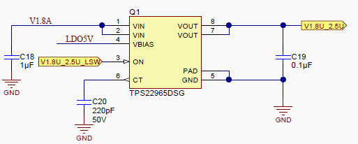
    If you checked our EVM and customer design regarding V1.8U_2.5U load switch, our VBIAS is from LDO5V, and customer's VDD is fro +5VSB(VR5 output).  To follow our EVM design, it seems they should just need to change VDD from +5VSB to LDO5V which is option 2.  Then, there's no need to have insert a 32ms delay between SLP_S$ and SLP_SUS, am I right?

    TI-EVM:

    Customer original design:

    Antony

  • Antony,

    If bias is taken from LDO5V, there is no need to change sequencing. The disadvantage is LDO5V cannot support higher current limit that is needed in customer design.

    VR5 does not have current limitations and adding delay will solve the issue. Is additional delay during turnoff an issue for customer?

    Regards,

    Jay

  • Hi Jay,

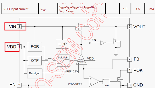
    Regarding options, they actually connect LDO5V to the VDD pin of the LDO as below.  So, it only consume 1.5mA max.  Do you think the current consumption here is still be a concern?

    The other concern is, they will connect this LDO output (2.5V) to VSB.  Currently it works ok.  Is it really necessary to add a resistive divider to generate 1.8V for VSB?

    Antony

  • Hi,

    One related question here.  Should all VSx level follow the table marked as below?  If this is true, VSB must be no bigger than 1.8 x 1.08 (typ)= 1.944V?

    For VSD, the nominal threshold is 1V for TPS650830.  If customer is using 0.95V, it seems easily to be out of the powergood range?

    THanks!

    Antony

  • Antony,

    1.5mA should not be an issue. In the schematic you had shown, i saw 0.49A and i was concerened.

    For VSB, i would suggest using resistor divider. In general, the comparator can be programmed to a window comparator which has both high and low threshold limits or level comparator which has only level comparators. i will double check and update you on VSB.

    For VSD, I expect there might be 0.1V voltage drop between output capacitor and VSD sense point under the PMIC due to traces.

    Regards,
    Jay
  • Hi Jay,

    Thanks. Please help us double confirm the acceptable votlage level range for VSD and VSB in TPS650830.

    Antony

  • Antony,

    I have double checked the OTP and confirmed it on bench. You cannot connect 2.5V to VSB pin. If 2.5V is connected, it will result in 1.8U_2.5U fault. You will need to check the power good status in register E7 as there is no power good pin for this comparator. PGB is used as qualifed enable and it will be high if ENB is high.

    Both VSB and VSD pin follow spec tolerance numbers.

    Jay

  • Hi Jay,

    Regarding VSD, so it would be very marginal if customer connect 0.95V_VCCIO to VSD.  Can they directly connect VR4 to VSD?


    Antony

  • Antony,
    Do you mean connect VR1(1.0V) to VSD? Yes, they can do it. VR4 is 1.2V and it cannot be connected. Please note that if VR1 is connected to VSD pin, PMIC will work properly but it would not monitor external VCCIO rail.

    Jay