This thread has been locked.

If you have a related question, please click the "Ask a related question" button in the top right corner. The newly created question will be automatically linked to this question.

TPS65000: TPS65000RTER abnormally damaged

Part Number: TPS65000

HI:

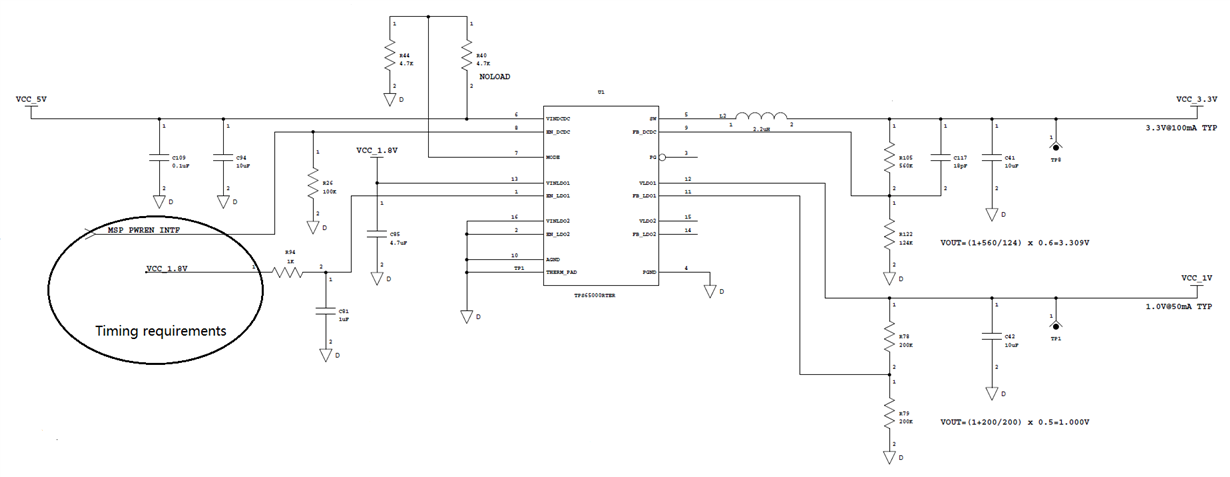
     Our products use the TPS65000RTER as the system power supply, from the product development stage to the final mass production stage, often encountered the chip damage situation(More than a hundred samples), the abnormal phenomenon is the chip fever, but the output voltage is still relatively normal, it is difficult to detect, but when the chip heat to a certain extent will affect the system other part of the work, the chip around the schematic diagram see annex, please help analyze the cause of the chip damage, thank you.

  • Hello,
    thank you for posting your question on the TPS65000 in the e2e forum.
    Your thread has been assigned to the expert within TI, who will reply to your question as soon as possible and attempt to resolve your issue.

    Regards,
    Eran.
  • Hi Yu,

    How exactly are the devices failing? There are no obvious mistakes in the provided schematic, and the currents are low enough that I would not suspect thermal issues.

    Best Regards,

    Rick S.

  • Hi Rick,
    We have produced more than 5,000 products, about 100 cases have the failing, More cases occur during the development process, often touching under power, So it has always been considered a problem caused by ESD, But the mass production stage products is not a good explanation of this failing, Because the ESD protection of the production line is good enough.
    Best Regards,
    Yu
  • Hi Yu,

    I cannot discern from your description what kind of damage the PMICs are incurring if not from ESD. Are the failure modes the same for all devices? Do they fail after any specific test?

    Best Regards.

    Rick S.

  • Hi Rick,
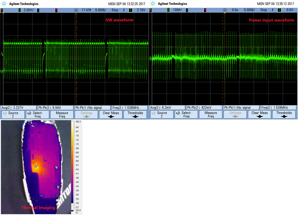
    The failure modes are same for all abnormal devices, The PMICs output voltage is normal, only the chip fever, And we did not do some special tests on the abnormal devices, In addition, I test the waveform of PMICs SW signal and power input signal(AC coupling), Found some exceptions, Please look at the waveform.

  • Hi Yu,

    These captures are very helpful, thank you :-)

    Since the buck should consistently be in PWM, it looks like it is being disabled every 20uS. How does EN_DCDC look during this behavior? If there is oscillation on EN_DCDC, an additional capacitor on this pin might be able to filter it out.

    The input voltage ripple would be most impacted by the ESR of the input capacitor, where DC bias derating could also be impacting performance.

    Best Regards,

    Rick S.

  • HI Rick,

           I test the EN_DCDC signal waveform, no abnormality found.

  • Hi Yu,

    Thanks for confirming this. In your schematic, R40 has "NO LOAD" next to it, does this mean that it is not populated? If so, does the device change behavior when forced into PWM mode?

    Best Regards,

    Rick S.

  • Hi Rick,

           The "NO LOAD" means not populated.

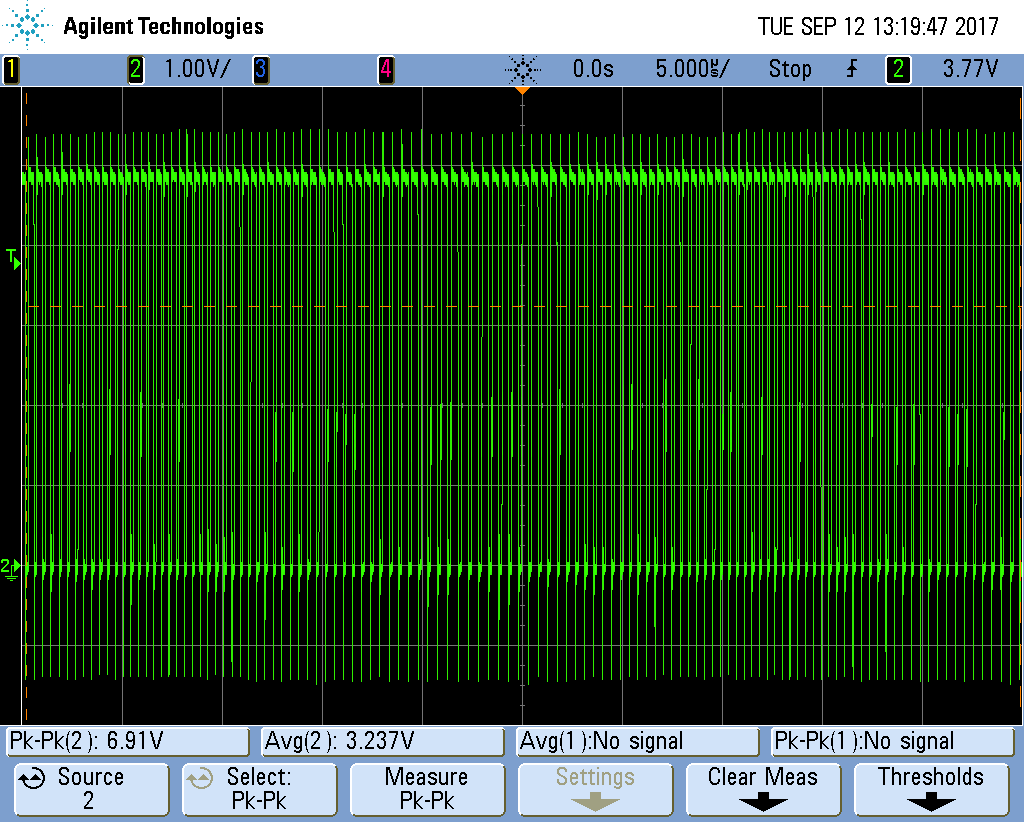
            I change the device behavior forced into PWM mode(delete R44 and add R40 with 4.7Kohm), the SW waveform back to normal, but the chip is still hot.

           So, you are right the SW waveform depending on device mode set.

  • Thanks Yu,

    If the load is constantly operating near the PFM to PWM transition point, you may see benefits from constantly forcing PWM. Do new devices have less thermal issues if you only operate in PWM mode? Also, have you been able to verify that the input and output capacitors have low impedance return paths to the device?

    Best Regards,
    Rick S.
  • Hi Rick,

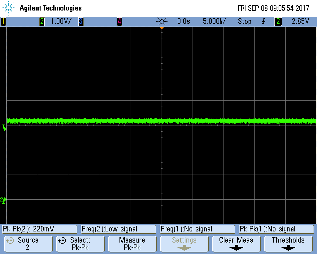
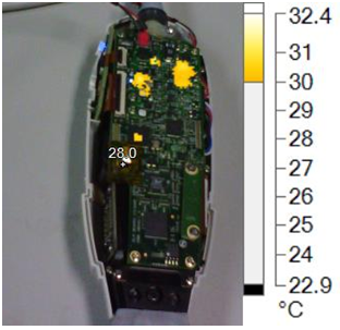
        The thermall issues is abnormally state, The new device does not have an abnormal thermal state in PWM/PFM automatic transition mode(only 28℃):

    The difference between the temperature of the new device and the temperature of the previous abnormal chip(83.3℃) is still very large.

    So I don’t think it is the difference caused by the device operation mode.

    Also, I have not figured out how to verify the impedance of the input and output capacitors, The actual design is using the X5R capacitor to guaranteed low ESR.

    I have replace the new capacitors to C94 C41, but the chip is still hot.

  • It sounds like the thermal issue follows the device once it is already damaged, and this can be confirmed by swapping the devices between known good and bad boards. If the behavior follows the bad device you may want to reach out to a local TI FAE for a failure analysis to confirm the failure mode.

    From a layout perspective, impedance can be affected by large loops connecting the capacitor ground pads to the device GND pins which can introduce unwanted inductance that may affect device performance. Additionally, while the devices are rated for component level ESD, they are not rated for system level ESD and can still be damaged if exposed to events once mounted to the board, especially while the device is operating.

    Best Regards,
    Rick S.
  • Hi Rick,
    Thanks for your support, I will contact local TI FAE for the failure analysis.