This thread has been locked.

If you have a related question, please click the "Ask a related question" button in the top right corner. The newly created question will be automatically linked to this question.

TPS65381A-Q1: When using DIAG_OUT as both MCU ADC and MCU GPIO

Part Number: TPS65381A-Q1
Other Parts Discussed in Thread: RM41L232,

Hi Please tel me.

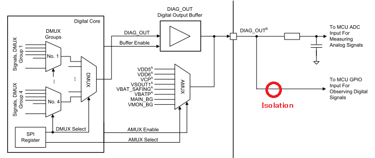
When using diag_out as both adc and gpio, it is written in the data sheet as shown below.

If the application must measure analog signals with an MCU ADC and monitor digital signals with an MCU GPIO, the
application design must assure the GPIO input stage does not affect the ADC measurements. If isolating the MCU
GPIO is not possible within the MCU, the application design must achieve the necessary isolation externally.(datasheet:34page)

When both are used, although it is written that GPIO is isolated, is there no problem if using an inductor?

Also please tell us the AD and recommended R and C constants.

  • Hello Otake-san,

    The word isolate may not be the best choice of description about this topic.  What was intended with this statement is that some MCU IOs have integrated pull up or pull down resistors or they have high leakage that would cause any analog output via AMUX to be in accurate because of the influence from the GPIO on the signal.  If the MCU used has a GPIO pin that can be high impedance and thus have no impact to any analog signal output via AMUX then it is fine.  I'm not sure an inductor would work because since at DC it would still allow the current to flow into the MCU if the MCU GPIO pin was not high impedance.  Normally in a case where the MCU is not high impedance a buffer with high input impedance could be used between the DIAG_OUT pin and the GPIO. 

    In most cases I have seen the MCU GPIO has a programmable or configurable pull up / down and high impedance option, so usually the GPIO can be correctly configured on the MCU itself.   

    Best Regards,

    Scott

  • Hi, Thank you for your answer.

    Place the buffer between DIAG_OUT using the pull-down GPIO pin.

    There is a low pass filter in front of the ADC pin, is it necessary?
    (MCU uses RM46L852PGE.)

    one more question,

    "In case one of the AMUX signals after the divide ratio is at a voltage above the VDDIO voltage,

    a clamp becomes active to avoid any voltage level higher than the VDDIO voltage on the DIAG_OUT pin."(datasheet,35page)

    →For example, when VDDIO is 3.3 V, doesn't it output more than this voltage?

    Best Regards,

    otake

  • Hi Otake-san,

    If the MCU IO pin cannot be put into a high impedance state then the bugger needs to be between the DIAG_OUT and the GPIO pin.  Whether or not a low pass filter is needed depends on the specific MCU and the ADC of the MCU, or other ADC that is connected.  We have a TID-Design, that uses a similar MCU, the RM41L232.  Below is the schematic capture for this TI Design and how the TPS65381A-Q1 DIAG_OUT is connected to the RM41 MCU.  The net going to TPS DIAG_OUT pin is called TPS_DIAG and is seen below.  This net goes directly to a GPIO that can be put into high impedance mode and then is connected into the low pass filter and the ADC channel.  The full design files and information of this TI Design are available at:  http://www.ti.com/tool/TIDA-00548


    To answer the second question, you are correct: when VDDIO is 3.3 V, the DIAG_OUT pin will not output more than 3.3V.  An example of this could be using the AMUX to output the VBATP level while VBATP is 34 V, the AMUX divide ratio for VBATP is 10, so 3.4 V should be put out on DIAG_OUT, however the DIAG_OUT output will be clamped to 3.3V.  The divide ratios have been selected so that generally the only time any clamping will occur is for battery related signals with very high battery input levels or a catastrophic short on the PCB such that a lower voltage rail such as VDD5 would be shorted to battery supply level. 

    Please let us know if you have additional questions.

    Best Regards,

    Scott   

  • Hi, Thank you for your answer.

    I understood about DIAG_OUT.
    Although the contents of the title and question are slightly different,
    are "VSIN", "VSOUT1", "VSFB1", "VTRACK1" open and okay?
    Best Regards,
    Otake
  • Hello Otake-san,

    When VSOUT1 is not used by your application is it okay to leave these pins floating, but normally we recommend to take VSFB1 to ground. We have an application note, the design checklist at:  http://www.ti.com/lit/pdf/slva611  which will help you double check the design implementation. 

    Please let us know if you have further questions.

    Best Regards,

    Scott 

  • Hi, Thank you for your answer.

    I didn't know the existence of the design chekclist.

    I solved it with this,thank you.