This thread has been locked.

If you have a related question, please click the "Ask a related question" button in the top right corner. The newly created question will be automatically linked to this question.

TPS65094: TPS65094 CH4 damage.

Part Number: TPS65094
Other Parts Discussed in Thread: IPG-UI, , TPS65086, TPS650864

Dear Sir

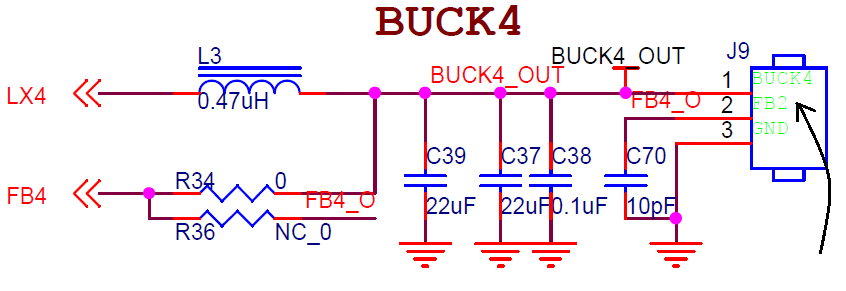
Please check TPS650941 circuit which is designed by my customer.

Conditions Vin = 6V and Vin = 12V

After downloading firmware, board power on make CH4 damage.

The pin24(PVIN4) become to 0 ohm. ( short to GND )

If enable CH3, the chip is not working

If not use the CH3 and CH4, the chip work normally with other channels.

Please help us to check what's problem.

Attached files are circuit and PCB layout.

tps65094x_EVM_v1.0.pdfTPS65094x_EVM_top.pdfTPS65094x_EVM_bottom_mirrored.pdfTPS65094x_EVM_top_silk.pdf

  • Thank you for your question. I need more clarification of the issue. When you mentioned DCDC4 is damaged, is it external component issue or PMIC issue. Can you double check if the external cap is shorted on DCDC4. Also, on the schematic you had provided, it looks like FBVR4 is labeled FB2. Can you double check.

    Are you enabling the rails by PMICEN pin and SLP_S4 signals? Can you also provide screen shots of DCDC3 output to check if the SW mode is trying to switch.

    Regards,
    Jay
  • Hi Jay :

    We checked the schematic several times.
    We didn't find any problem.
    You say "it looks like FBVR4 is labeled FB2"
    means the schematic shown below ???
    If it is true, R36 open make FB4 dosen't connect to FB4_O.

    I think is PMIC issue. Is it possible the problem comes from soft?
    The soft download from TI link, right ?
    http://www.ti.com/tool/ipg-ui

  • the chip is tps 650941 k 1 it looks like FBVR4 is labeled FB2. Can you double check.// i did not found FBVR4 ,,Whether does the FB2 mean the FBVOUT2 ?

    2Can you double check if the external cap is shorted on DCDC4//no short
    3 Can you also provide screen shots of DCDC3 output to check if the SW mode is trying to switch//What is it ?
    4 .Are you enabling the rails by PMICEN pin and SLP_S4 signals?//YES see the r1 and r5 in the sch
    5 by the way if the pgnd_buck3 and pgnd_buck4 are not well soldered to system dgnd of board , whether will it result the error of buck3 and buck4 But the buck5 is working well

    6 there is no switching signal with buck 3 when set the vr_ctrl1 register to 0X27 , set the vr_ctrl2 to 0XB7
  • 1. I think the FBVR4 Jay is referring to is the J9 jumper that you pointed out. It looks like the wire is labeled correctly so I don't think it should cause an issue. From what I can tell it looks like it is connected correctly in the layout as well.

    2. Can you check C4, C6, and C20 as well as C5? All of those caps are connected to the PVIN4 pin through the VIN_BUCK345_ANA net so if any of them are bad it could cause a short on PVIN4.

    3. The switch node Jay is referring to is LX3.

    5. When you say pgnd_buck3 and pgnd_buck4 do you mean the ground connections to their output caps? I don't see any pgnd_buck3 or pgnd_buck4 in the schematic. Also if PVIN4 is shorted then I would expect BUCK5 shouldn't be working either. BUCK3,4,5 are all connected to the same supply so if the input to one was shorted then they should all be shorted.

    I don't think it would be a software issue. If you can send a register dump from IPG-UI after the issue occurs on BUCK3 that might help us identify what is happening.

    Thank you,
    Nick
  • 1  yes  FBVR4 connection is ok  

    2 The c4 ,c6,c20 and c5  are  ok 

    3 There is no switching signal  with lx3

    4 The  pgnd_buck3 and pgnd_buck4  are  drew   in the block   diagram  of  tps65094x

    5 when enable buck3., the Other bucks  arenot working ( include buck1,2,,5,6)

    6 when 3 channel buck is not enabled , the buck 1.2..5 are ok 

    7  when the initial code downloaded .The channel 4 buck is  enabled  for some  seconds ,then the  4 buck  is always short  .  so two boards are burned off  with the chip , . We must cut the buck4 input power  trace  with other boards

    6 can you send the tps65094x initial code to us .  we want to compare it  with our code 

    thank you 

  • The best place to see what the initial code is for the device is to look at the datasheet in section 6.7 "Register Map". This shows what all of the registers should be set to as soon as you turn on the device.

    www.ti.com/.../tps65094.pdf

    You can also connect to the PMIC and click the "Read All" button in IPG-UI and then go to Report>Dump Registers to create a file with all of your register contents. This would help us see what the PMIC is reporting after the issue occurs.

    I would also check to see if LX3 is getting shorted to GND. I am not sure how that would cause PVIN4 to short to GND, but it might explain why turning BUCK 3 off causes the other BUCKs to work.

    Thank you,
    Nick
  • 1  According to the  spec ,write the  registers ,Because other bucks are  good ,but   the 3 buck and 4 buck  .are bad  What  is the writing  register sequence for tps65094*? please send it to us

    2 There are no  read button and IPG_UI  ,can you send the initial code of  TPS65094* to us? or you can download the dump registers from the IPG_UI  to us ?

    thank you .

  • There isn't a default register writing sequence. The registers are written during manufacturing to default settings that should be there as soon as the device is turned on. Just in case there is an issue I took one of our EVMs, read all of the registers and put them into a register dump for you to compare to your device. 

    E2E_regdump.txt
    RegAddr		Value
    01			29
    02			08
    03			FF
    04			00
    05			04
    20			38
    21			00
    22			11
    23			11
    24			00
    25			0C
    26			0C
    27			00
    28			3C
    29			0C
    40			55
    41			55
    42			05
    43			07
    91			00
    92			80
    93			80
    94			2F
    95			2F
    96			4B
    97			4B
    98			47
    99			47
    9A			AA
    9B			BB
    9C			07
    9D			02
    9F			70
    A0			00
    A1			20
    A2			C0
    A3			37
    A4			E7
    A5			FF
    A6			FF
    A7			FF
    A8			DF
    A9			3F
    AA			C6
    AB			3F
    AC			FF
    AE			7C
    B0			FF
    B1			69
    B2			00
    B3			00
    B4			00
    B5			00
    B6			00
    

    I also put these registers into a project file so you can open this project, and then click "write all" to set all of your device's registers to the default values.

    E2E.json

    To send us a file with your register dump you can follow the pictures below.

    Thank you,

    Nick

  • 1The  *.txt file is about the  tps65086? Whether does the tps65086 comptabile with  the  TPS65094? 

    2  we checked the register  ,which mee the spec  .

    can you send the  TPS65094"S setting to us ?

    thank you 

  • I just did another register dump to confirm this register dump is from the TPS54094.

    The TPS65094 is the same device as the TPS65086 with a different OTP. When you start a new project in IPG-UI, you need to select "TPS650860-1.1" as the device.

    If you could send a register dump from your device after the error occurs on BUCK3 I can look at what the PMIC is reporting as the issue. Also, have you tried probing the LX3 pin to see if it is shorted?

    Thank you,
    Nick
  • hi nick:
    we does not use the PMIC , The registers are downloaded by our system system, there is no signal with lx3 ,when enable en1---5.
  • I am not sure what you mean when you say the registers are downloaded by your system. Do you not have access to them? Reading those would help out a lot.

    Also, when you say there is no signal on LX3 is it being shorted to ground? If so is it only on the boards that have been damaged, or is it also true on an unused board?

    I also looked at you schematic again and noticed a couple issues.
    1. BUCK2 inductor value is over the maximum inductance
    2. BUCK2 output capacitor is below the minimum capacitance
    3. BUCK3 output capacitor is below the minimum capacitance
    4. BUCK4 output capacitor is below the minimum capacitance

    You can look at the datasheet to see all of the minimum and maximum values for these components. It would be a good idea to replace these with components that are within the specs.

    Thank you,
    Nick
  • hi  nick:

    1 The  tps65094X is used in our system  ,so our chip   OV **  can write or  read  the TPS65094*   register by  i2c  

    2   There is no signal  with  LX3  ,which means  enable the LX1 ,LX2, LX3,LX5,LX6 ,but  there are no output signal  with all the  bucks . but  when  only  enable  with the lx1,lx2,lx5,lx6  ,the LX1 ,LX2,LX5,LX6 are ok , and only enable the LX3 single  ,the LX3 is ok  .so LX3 is confused with other BUCKS

    3 changed the buck2 inductor  and buck3 output capacitor, the result is same as before 

    4 can you  give some suggestion  about it ? or we mail one board to you ,you can help us to debug it ?

  • Ok I see what you are saying. If you could read the SHUTDNSRC register (address 0x5) and PWR_FAULT_STATUS registers (address 0xB2 and 0xB3) after the BUCKs stop working and send me the results that would be great.

    I would also try probing the VIN_BUCK345_ANA pin to check for any voltage spikes, as well as the switching pins for any ringing that may be causing damage. If you could get a screenshot of these to send me that would be very helpful.

    I would rather try to solve this remotely if possible.

    Thank you,
    Nick
  • HI NICK :

    0x5=00h.0xb3 =  00 ,0xb2 :buck3 ,buck4  ==1  I


  • Were you able to probe the input to see if there were any voltage spikes or the switching pins to see if there was any ringing?

    Thank you,
    Nick
  • hi  nick:

    1 we use the standard  6v  input 

    2  There is some  ringing  or   howling  from  inductance ,  when  enable the buck4  for some seconds  ,  then  The buck4  is shorted  quickly

    by the way   ,if the buck4 's  FB is unstable  ,which will  lead  to  buck4  destory   

  • Would you be able to show me a scope shot of the ringing on the switching pin? If there is ringing it is possible that it is causing the switch node voltage to go higher than it should, and could damage the device.

    Thank you,
    Nick
  • hi nick :

    we got the samples tps640941 ,changed it  , but the buck4 is not woking  ,We found that  the PMIC=1  ,There are more noise  pluse on  the inductors of buck4  without enable  buck4

    The belowing picture is the noise pluse 

    thank you

    M erry christmas


  • Hello,

    Are you using this device to power an Intel Apollo Lake processor?

    When setting PMICEN to '1', BUCK4 is enabled by default for this part number. Please see Figure 6-7 in the datasheet which shows the sequence. Also note that when PMICEN is low, all rails are disabled, regardless of the I2C_RAIL_EN register setting.

    If you are not using this device with an Intel Apollo Lake processor, I would recommend using the TPS65086 or TPS650864 family instead. There are Intel specific features enabled in the TPS65094 that may interfere with using it in another way.
  • hi  kevin :

    thank you 

     no   The power   chip   is  for  new  Omnivision ASIC processor,  The power sequence is fellowed  ,according to the SPEC  .When PMICEN  and buck4 are enabled for some time  ,  The buck4 's inductor  become buzzing for  some time    ,then the chip is damaged ,which become short .


    The  attchment is our sch and layout  ,  Whether is the  two layers board not for  the power?


    tps65094x_EVM_v1.0.ziptps65094x_EVM_v1-0928-1.zip1325.tps65094x_EVM_v1.0.zip


  • Hello,

    Thank you for the board file, it is much easier to navigate than the PDF and makes it more clear. I have not seen someone do a 2 layer board design with this part; in looking it over I am a bit concerned regarding the parasitic impedance on the GND return path for all 3 BUCK converters. In particular, all three of the converters are going to end up funneling into a small area between the DRV input and FBVOUT1 or around the other edge of FBVOUT1. See the image below. 

    Can you check the switch node in a scope shot? I am concerned with how high the ringing might go. With the added impedance, it may be ringing higher than expected. Note that this will require a high bandwidth scope to be able to see.

    Finally, I would still recommend switching to the TPS65086 or TPS650864 family; they provide better catalog control than the TPS65094 family. With the TPS65094, if the part has a power fault after you change the default voltage settings then the voltage will power-up again to the pre-programmed value because PMICEN is high. For the TPS65086 or TPS650864 family, the CTLx pins can all be set to GND and a power fault will just cause all rails to turn off.

    There is a good article regarding the impacts of parasitic impedance here: 

    Note: highlighted red boxes are the input and output capacitors located on the other side of the board.