This thread has been locked.

If you have a related question, please click the "Ask a related question" button in the top right corner. The newly created question will be automatically linked to this question.

TPS659039-Q1: LDO2 & LDO3 rise time issue

Part Number: TPS659039-Q1
Other Parts Discussed in Thread: DRA756, DRA75, TDA2

Hi,

We are using TPS659039 for DRA756 power and we see that all the power sequencing is as per recommendation in datasheet. 

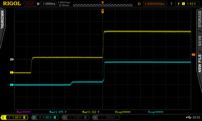
But for LDO3 and LDO2 we see unusual raising with some glitch. 

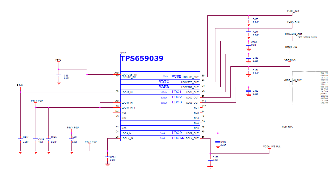
As per my knowledge we have followed all design rules recommended by TI for TPS659039. Attaching the oscilloscope capture for LDO3 and LDO2 power. Please guide us what could cause this issue and how can we resolve it?

Note: Channel 1 - LDO2,  Channel 2- LDO3


Regards

Bharati

  • Bharati,

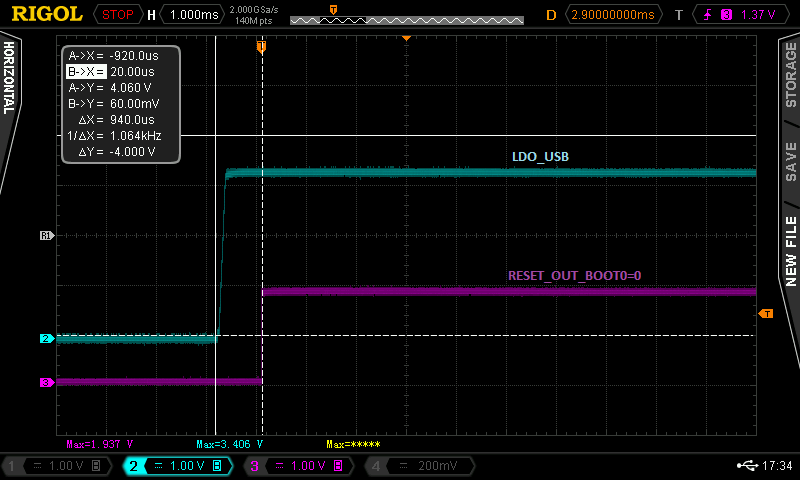
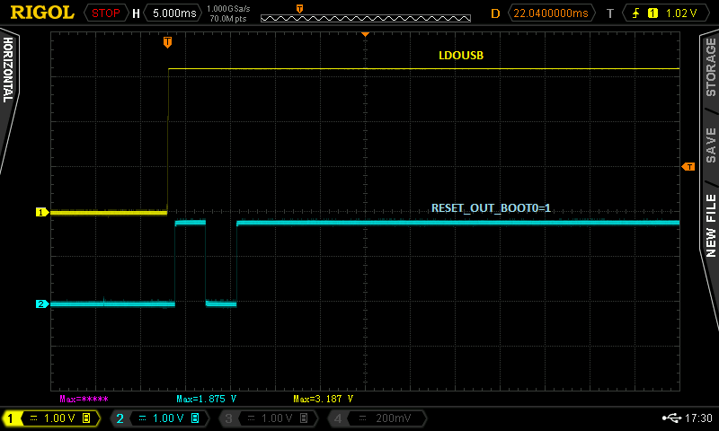
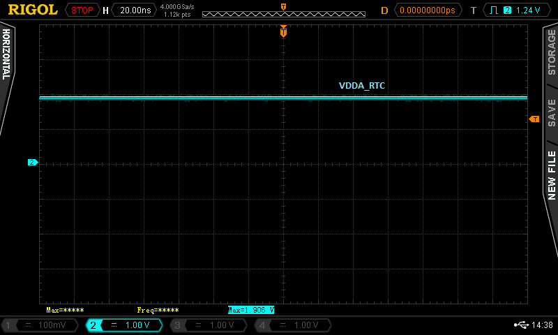
    Can you also probe RESET_OUT and VRTC? Additionally, can you share your schematic for LDO2 and LDO3 (input and output)?

    Thanks,

    Nastasha

  • Hi Nastasha,

    Attaching the captures for RESET_OUT and VRTC.

    RESET_OUT is captured with respect to LDOUSB signal. I have captured for both Boot0=0 and Boot0=1 

    Attaching VDDA_RTC signal and ripple captured for VDDA_RTC.


    Regards

    Bharati

  • Hi Nastasha,

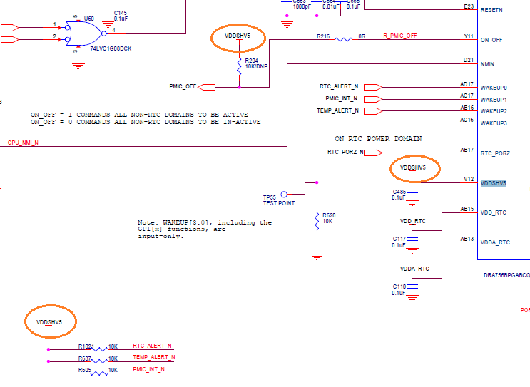
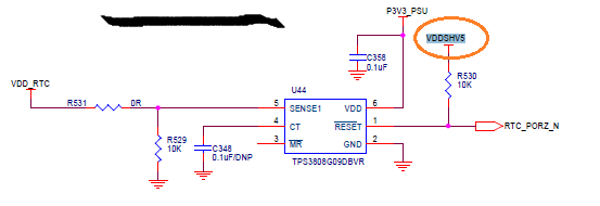
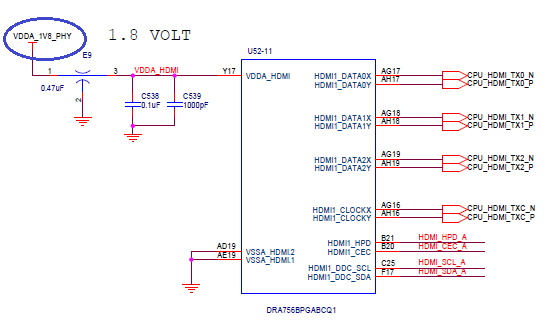
    Here is the schematics for LDO2 and LDO3. 

    > LDO2 is named as VDDSHV5 and it is connected to following circuits 

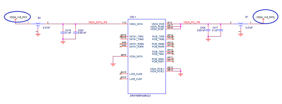
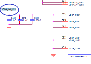
    > LDO3 is named as "VDDA_1V8_PHY" and connections are as below

    Please let me know if you need any clarification on connections

  • Bharati,

    Thanks for providing your schematic and scope shots. I am looking into this and will get back to you shortly.

    Nastasha

  • Bharati,

    LDO3 is okay, there is more information about this expected behavior in the DRA75 errata documentation (item i939).

    LDO2 is a 3.3V supply that looks to be turning on too early, causing a power sequence violation. Thus, it is being clipped by internal diodes.

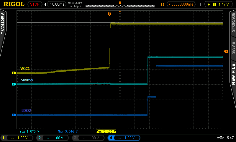
    Is there a location in your design where VDDSHV5 is connected to a VDD_1V8 rail? Can you also take a scope shot of LDO2, VCC1, and SMPS9?

    Thanks,
    Nastasha
  • Nastasha,

    1) Thank you we will look into errata for LDO3 behavior.

    2) For LDO2 , I have confirmed VDDSHV5 is not connected to any VDD_1.8V  in our design.

    Attaching the captures for LDO2, VCC1 and SMPS9. Seems like when SMPS9 is rising, LDO2 is trying to go high but as you mentioned it is getting clipped by internal diodes.

    In what case is this behavior expected.? How do we resolve this?

    Regards

    Bharati

  • It is likely the circuit connecting to LDO2 is connected to a 3.3v circuit, which is powered prior to the LDO2.  The 'step' voltage is approx 1 volt due to diode clipping.  I recommend reviewing the design to ensure no peripherals connected to LDO2 (or VDDSHV5) are powered and/or driving IO into VDDSHV5 bank prior to LDO2.

    Thanks
    Robert

  • Hi Robert,

    As you see in my previous mail, I have attached screenshots of VDDSHV5 connection in our schematics. As you can see LDO2 output is directly connected to DRA756, VDDSHV5 pin with 0.1uF cap and 4 pull ups are connected to VDDSHV5 power supply. It is not connected to any other circuit. To make sure there is no other circuit connected to VDDSHV5, I have removed 4 pull ups as well from the board but still the LDO2 output has 1.8V step voltage before rising to 3.3V.

    Regards

    Bharati

  • Bharati,

    Power is the programmed power sequence?  Is LDO2 (3.3v) ramped at same time as SMPS9 (1v8)?   If yes, this is is a violation of the power sequencing requirements.  3.3v IO are not allowed to ramp until after 1v8 and the AVS/Core supplies are ramped.  See the power sequence diagram in manual.

    In the design, what are the following pins connected to?

    (ON_OFF, RTC_ISO, RTC_PORZ, WAKEUP[3:0]? 

    These are the VDDSHV5 IO.  I was suggested the peripherals connected to these IO are likely powered, and driving current into the un-powered IO, thus leaking onto the power domain.  The DRA75x device does not support fail-safe IO, and thus this is a violation of the spec.

    Thanks

    Robert

  • Hi Robert,

    As mentioned in earlier mail, LDO2 is not rising to 3.3V completely when SMPS9 is rising but there is step voltage at LDO2 when SMPS9 is rising.


    >ON_OFF: Pulled down to ground with 2K.
    > RTC_ISO: Connected to AND gate output and PORZpin of DRA756. AND gate is powered with 3.3V from external DCDC (Same in EVK as well).
    >RTC_PORZ: pulled up to VDDSHV5
    > WAKEUP[0-3]: pulled up to VDDSHV5

    I am disconnecting peripherals whose signals are pulled up to VDDSHV5 to make sure there are no peripherals connected to it.
    We will check if it resolves issue.


    Regards
    Bharati
  • Hi Robert,

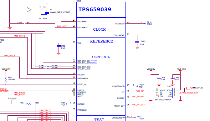
    We removed  IC's connected to VDDSHV5 one by one and found that LDO2 step voltage is not there when we remove Level translator (U101) connected to PMIC_INT signal. Attaching screenshot for reference.

    We have connected VDDS18V at Channel B and P3V3_PSU at Channel A which is same as that of EVK. We are using TPS53515RVET buck regulator to convert 12V to P3V3_PSU and it comes up as soon as board is powered on and same is connected to PMIC LDO input.

    In our design we also have load switch between P3V3_PSU to P3V3 and we observed step voltage issue is resolved when we connect P3V3 instead of P3V3_PSU to voltage level translator channel A.

    This is surprising because EVK also has PS_EVM_3V3 as input voltage for PMIC LDOs and same is connected to level translator channel A for PMIC_INT. For our understanding could you please explain why step voltage is seen in our application but not in EVK. We would like to understand if we are missing out on something.

  • Bharati,

    I know the TI's EVM has leakage issues early on as well - for similar reasons you are experiencing.  However - I thought they got resolved.  I'll need to go back and pull the data.  Without question - the level translator on for the PMIC_INT signals should be powered on the VCCA side by the same rail as the TDA2 IO.  If connecting to one of the WAKEUP signals, then is should be powered by same power rail that powers VDDSHV5.  This will resovle the leakage caused by PMIC_INT.  

    Thanks

    Robert

  • Hi Robert,

    We resolved issue by connecting VDDSHV5 to PMIC_INT level translator channel A.

    Thank you for your support.


    Regards
    Bharati