This thread has been locked.

If you have a related question, please click the "Ask a related question" button in the top right corner. The newly created question will be automatically linked to this question.

Questions about LM5060-Q1

Other Parts Discussed in Thread: LM5060-Q1, LM5069, LM5060

Hello,


I have some questions about LM5060-Q1.

1.Please let me know the guarantee tolerance dose of the body Diode of SENSE, nPGD, UVLO, and an OVP pin.

  Both of forward current and backword current.


2.Please present the detailed data of the VIN=5V neighborhood about the datasheet 6 page figure3 VGATE vs VIN characteristic.


3.Please give me proposal of the protection circuit which can cope with the protection to negative serge, and power supply reverse connection protection.

  The condition of negative serge is followed as:

  ・Voltage : -600V     ・Period  : 1msec      ・Repetition : 5000times           ISO7637-2


  • Hi Yoshida-san,


    I would be glad to help you with these questions:


    1. Can you elaborate on this question as I had trouble understanding. Are you asking for the normal operation electrical specs, or ESD structures on those pins of how much they can sink or source during an ESD event?


    2. I am looking into this to try to find the original data.


    3. We have application notes on our LM5069 product page under "Technical Documents", copied here:


    Surge Stopping and Reverse Voltage Protection with the LM5069

    http://www.ti.com/lit/pdf/snva683


    as well as:

    Stopping Reverse Current Flow in Standard Hot Swap Applications

    http://www.ti.com/lit/an/snva673/snva673.pdf


    These application notes should provide a background of the additional circuitry used to protect against surges and reverse current in hot swap applications. However, we have not tested these circuits to such extents of -600V for 1ms, 5k repitition that the ISO7637-2 standard requires.


    Thanks!

    Alex

  • Hi Alex,


    Thank you for your reply.

    The question of No. 1 relates to the question of No. 3.

    I would like to know the current which can be sent momentarily.


    There is a question by addition about the question No. 3.

    Can LM5060 be driven even if it replaces the direction of NMOS  Q1 and Q2 of Fig. 38 of a datasheet?

    It is because D3 (Zener Diode for load dumping protection) can be inserted between Q1 and Q2 and D2 (for adversative conjunction protection) becomes unnecessary.


    Yoshida


  • Hi Yoshida-san,

    1) This device can support a 2kV ESD HBM rating according to standard JESD-22-A114-C as indicated on page 3 of the datasheet under "Absolute Maximum Ratings". Let me know if this answers your question.


    2) I sent in the request to our test verification team to obtain this original data. Because it is a formerly National Semiconductor device, it is not in our typical database.


    3) I am not familiar with implementing such a configuration and will need to consult with our team for further advice.


    Thanks!

    Alex

  • Hi Alex,


    About the Question 1), in this case I would like to check whether it is satisfactory, when a negative serge pulse is inputted into these pins.

    Here, with the negative serge pulse, it is proportionate to ISO7637-2.

      The condition of ISO7637-2 is that voltage is -600V , period is 1msec and repetition is 5000 times.

     I don't understand this condition for whether I may think that it is the same as ESD.

    Your reply is right if that is right in this case.

    If that is not right, how much is ability?

    I would like to know whether it is a thing which needs the measure by a protection circuit.


    By that, a question is asked about the protection circuit with the question 3.


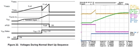
    Operation with the system was checked about the timing of Vds and a Vgs comparator of operation.

    As a result, in order that a Vds comparator may work previously, it does not become as the normal standup sequence which has a statement in a datasheet. (see a figure)

    - May I judge that it is normal as operation?
    - When an order changes, aren't we anxious about some?
    - If the above-mentioned operation is judgment of being normal, what kind of state is the sequence of the figure the motion supposing?
    Please let me know about the three above-mentioned points.


  • Hi Yoshida-san,


    1. Our device has never been tested under -600V conditions for 1ms periods as the ISO7637-2 requires. We cannot guarantee operation beyond our absolute maximum ratings specification in the datasheet.


    2. Can you tell me more about your application and why you are interested in the 5V region within Figure 3? Note that the device specification is a minimum of 5.5V for VIN for the LM5060.


    3. We have not used FETs in this reverse direction and therefore cannot judge whether the operation observed is normal. Can you tell me why you are trying to use the FETs in this way?

  • Hi Alex,


    1. I understood this situation.

      Do I hear that it is necessary to cope with it in an outer protection circuit?


    2.What I care about most is the gate voltage at the time of power supply starting.
    I want gate voltage to be over 10V in the hit which the power supply rose and exceeded the threshold value in the 5V neighborhood.


    3.The reason I would like to change direction of the drain-source of FET(Q1 and Q2) such is because it thinks that D2 becomes unnecessary since the zener diode of D3 can be put in between Q1 and Q2 of Fig. 34 of a datasheet.


    How is the waveform asked by the addition?

    Is this operation is normal?


  • Hi Yoshida-san,

    1) Yes, our device would likely fail if it is subjected to -600V, 1ms duration, 5000 repititions as this is a high stress condition. An outer protection circuit would be needed.


    2) Will you be using the UVLO functionality of our circuit? If so, then I would suspect the device will remain off until the input voltage is within the LM5060's operating range. Therefore the VIN = 5V would not play a role in the gate voltage.


    3) The waveform shown looks like normal operation, however we have not tested this device with back-back FETs facing the opposite direction. This may be an area for us to test in the future, but at this time we have no information as to whether this will cause undesirable failures.


    Thanks,

    Alex

  • Hi Alex,


    1) I understand well that an outer protection circuit.

      If the optimal protection circuit is known, please let me know.


    2) Of course, he plans to use UVLO of a circuit.

     I want to know what volatage of the Vgate when a circuit begins to move by start-up exceeding 5.1V.
    Isn't there any detailed data in which the GATE voltage  begins to rise at figure3 of a datasheet?

    Near Vin is 5.1V neighborhood.


    3) The waveform is measured by direction of the usual NMOS Q1 and Q2 like a figure34 of datasheet.

      Although it is what this waveform is normal, figure24 of a datasheet differs from a sequence.
    Is what differ assumed?  


    Thanks,

  • Hi Yoshida-san,


    1. We have not tested protection circuitry for ISO7637-2 and thus do not have an optimal recommendation at this time.


    2. What is the input voltage range for the application? If the UV is above 5.5V, then the device will keep the 2.2mA pull-down on the gate until UV is passed.


    3. Are you asking if we can assume that the modified circuit will produce the waveform in Figure 24 of the datasheet, based on the test result you provided for Figure 22? We cannot assume the circuit will behave as desired without testing the modified circuit design for these conditions.


    Thanks,

    Alex

  • Hi Alex,


    2) The Typical input voltage is 12V.

         The input range will be set to 16V from 6V.

      When UVLO is set as 5.5V, is the gate voltage after PowerOnReset compensated for more than 10V?


    3) Sorry, my last explanation was wrong.

      A right waveform is a recommended circuit as shown in Fig. 34, and it expects and acquires a waveform as shown in Fig. 22.

      However, operation is different if Fig. 22 is compared with an actual waveform.
         Specifically, it seems that there is no fault period. 
         What is assumed as for the cause of this difference?


      ch1:Vtimer    ch2:Vgs  ch3:nPGN  ch4:EN


    Thanks,

  • Hi Yoshida-san,


    For 2) I will test this in the lab on an EVM and provide the results.


    3) I am having trouble analyzing the waveform, but first I would not recommend using the back to back FETs in this way. The reason is that the FETs no longer have their source pins tied together, and therefore Vgs is not equal and controlled. For example, you can easily apply reverse voltage to Vgs and cause damage to a MOSFET.

    8510.LM5060 Back_Back_FET.pdf


    As you can see, there is no protection for Vgs of the first MOSFET. The second MOSFET has the internal zener diode which can protect Vgs. In a typical back-back FET implementation, the sources of each FET are tied together and therefore protected by this zener.

  • Hi Yoshida-san

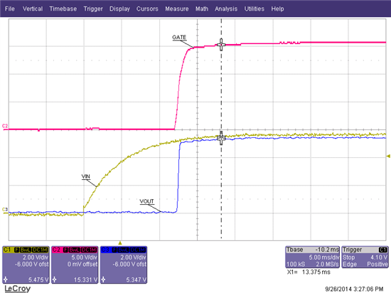
    2) I went in the lab and measured the gate voltage on an LM5060 where UVLO was disabled (tied to VIN).

    As you can see from the attached waveform, when VIN reaches ~5.475V, the Gate voltage already reached 15.331V (when measured with a multimeter after stablized, with VIN = 5.573V, VGATE = 15.745V)


    3) Also be aware that you mentioned the VIN range goes to 16V for your application, which means that the Vgs could be -16V with the gate disabled, using the modified circuit we discussed. However if you have any transients on the input, it could be worse and possibly damage the FET.


    Thanks,

    Alex