This thread has been locked.

If you have a related question, please click the "Ask a related question" button in the top right corner. The newly created question will be automatically linked to this question.

LM25066 power limit when output is short

Other Parts Discussed in Thread: LM25066

Hi,

I have one question about LM25066 as below.

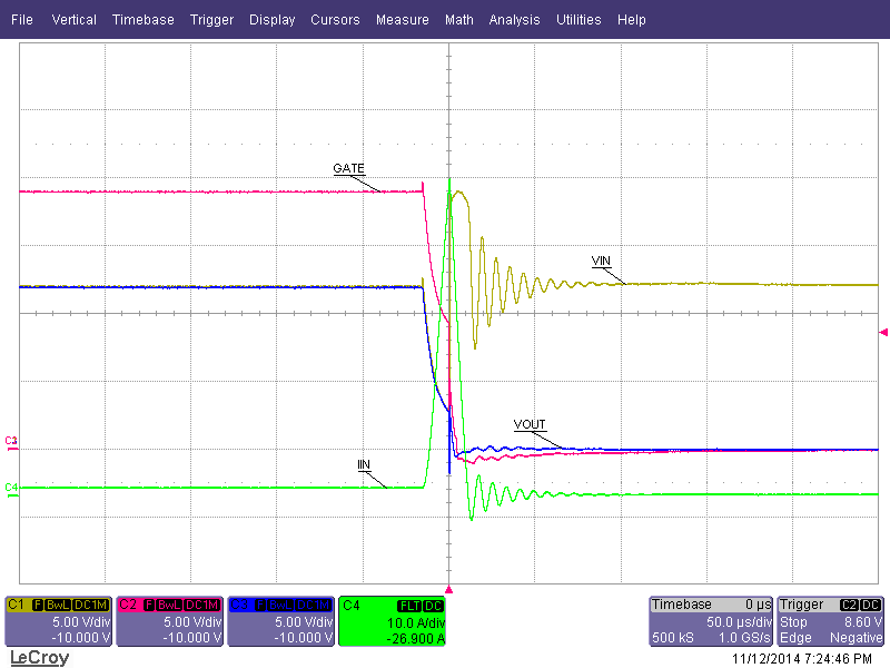
When output is short, is power limit effective here? Please see below waveform of output short test.

CH1:VIN  CH2:VOUT  CH3:TIMER  CH4: Iout(5A/V)   M1: MOS Power (Vds*I)

Power Limit set: 111W

Current Breaker set: ~23A

From waveform, after output is short, maximum MOSFET power is >111W, and maximum current is just ~23A.


Thanks.


Johnny

  • Hi Johnny,


    Do you know what the units and scale (how many Watts / division) M1 is?


    I had some trouble following the waveform since C4's offset is off the page, but it would help to interpret M1 and even have a waveform of the gate if possible.


    Thanks,

    Alex

  • Alex,

    From scope curve measurement, the maximum power of M1 is ~275W. C4 "zero" line is the same position with C1. CH4: Iout(5A/V)

    From device design feature, will power limit be effective when this kind of output short happens?

    Thanks.

    Johnny

  • I see it now, thanks Johnny.


    So the device is not going into power limit in this waveform. What you are seeing is that M1 is not showing the power through the FET, but rather the energy which is going into the TVS and being clamped.


    The input current to the right of Vout = 0 is nearly all into the TVS, and Vin being held nearly constant at 18.5V (with minor LC ringing) is the clamped voltage for that current.

    If the device is setup for retry, then later in the waveform you will see the device try to power back on, and at that point, it should be hitting power limit if the load is still shorted and you would see the timer pin begin to activate (and then fault out) when that occurs.


    Thanks,

    Alex


  • Alex,

    M1 calculation equation in scope is (VIN-VOUT)*IOUT, I can not understand "M1 is not showing the power through the FET, but rather the energy which is going into the TVS and being clamped". Could you explain it more clearly?

    And according to what you mean, if we remove input TVS, will M1 be clamped at setting value 111W?

    Thanks.

    Johnny

  • Hi Johnny,

    So what is being plotted looks like Vin Vout, IIN and the timer.


    IIN is equal to IOUT during normal operation, but when a hot short occurs, the gate will shutoff and therefore the current through the FET is equal to 0A.

    They should not probe IOUT, or else they will be seeing the current surge from the output capacitance into the short, not the current through the FET.


    So now IIN has to go somewhere. It cannot change immediately because there is some parasitic inductance in the traces. So it has two places to go: the input capacitance, or the TVS.


    If no TVS is installed, the current will go into the input capacitance and cause a large spike on VIN, which will surpass VIN ABS MAX and cause damage to the device. In addition, it will now serve as an LC circuit and begin to oscillate, likely dipping below GND and causing VIN to go negative.


    With the TVS installed, it will absorb most of the energy from IIN. The TVS will take this energy and clamp the input voltage below its ABS MAX (this can be seen in the second half of the waveform, where VIN is roughly constant at 18.5V. There is still the LC ringing, thus the minor oscillation, but it is minimal because of the TVS.


    Because the voltage across the TVS is VIN - 0V, this is roughly equal to the voltage plotted for the FET (VIN - VOUT) since VOUT = 0V after the hot short. Thus the power, M1 being shown is roughly equal to the power being dissipated in the TVS.


    I realize it can be difficult to explain without diagrams showing the current flow. I can draw up a diagram which may help to understand, but it would take a week as I am OoO the first half of next week.


    Thanks,

    Alex

  • Alex,

    Thanks for explanation.

    The current in waveform is IOUT to load, not IIN, which I have confirmed with customer.

    On my understanding, when output is shorted, VOUT drops to zero, at this time, gate sinking current is 190mA. But in waveform, the VOUT drop very fast (time scale is 1.0us/div in waveform). So the power limit circuit cannot control gate voltage to control FET power.

    Please reply your idea here?

    Thanks.

    Johnny

  • Alex,

    Any reply and comments is welcome.

    Thanks,

    Johnny

  • Hi Johnny,

    What is being plotted is Vout, not Vgate. If Vout is being hard shorted to ground, it's voltage will not follow Vgate's but rather will go to zero quickly. It depends on where it is being probed, output capacitance and parasitic resistance and inductance.

    If the customer would like to see the 190mA pull down of the gate, then the best way would be to view the gate waveform.

    The hot swap is not regulating power limit in the waveform (if it was, it would begin charging the timer cap).

    Thanks,

    Alex

  • Alex,

    In below waveform, CH1:GATE   CH2:VOUT, all voltage is test on EVM's test point.

    It seems the (GATE-VOUT) voltage has dropped to zero. For parasitic parameter influence, do you mean it's better to probe VIN and VOUT voltage directly at drain and source side of external MOSFET?

    Thanks.

    Johnny

  • Alex,

    Below is latest test waveform from customer.

    CH1VDS  CH2GATE    CH3TIMER   CH4:IOUT, 5A/V    M1:CH1*CH4*5(5A/V)

    VDS is test with differential probe. GATE is test at MOSFET side. IOUT is test at load side.

    From waveform, the maximum value of M1 is 313W. The maximum value of CH1 is ~20.5V, and CH4 is (4.57*5=22.8A).

    Below is the GATE-VOUT waveform.

    CH2:GATE   CH3:SOURCE  CH4:IOUT    M1:CH2-CH3 (GATE-to-SOURCE voltage)

    GATE and SOURCE voltage is test at MOSFET side.

    From above waveform, when VOUT drops to zero, GATE-SOURCE is 0.4~0.5V for 1us.

    From all test result, we come to a conclusion that when VOUT is shorted, GATE sink current is 190mA and power limit is not effective.

    Please give your suggestion and comments here.


    Thanks.

    Johnny

  • Hi Johnny,


    I will take some waveforms on an EVM in the lab to share the results. I suspect that the current shown above is not an accurate representation of the current through the FET.


    Thanks,

    Alex

  • Alex,

    Please use E-load to drive 1A IOUT and use "short" function for test. Appreciate your time.

    Thanks.

    Johnny

  • Hi Johnny,

    So depending on your e-load and setup (such as slew rate programming or using the "short" function versus a physical short), you may see slightly different results.


    This tests shows the current from IIN. This gives an accurate representation of the current through the FET until the gate turns off. At this point, no current will pass through the FET, and the current shown after this point is simply energy which is being absorbed by the input TVS.


    This waveform shows the output load which is regulating the current to 1A. In terms of wires/location, the short was applied just before the E-Load connection.


    This last waveform was taken and shows the current going through the wire which is being used to short circuit.

    As you can see, there is a large amount of current which is continues to decrease after the gate pulls low. This current is the energy being discharged from the output capacitors.


    In order to show the true power across the FET during a circuit breaker, you would need to remove the output capacitors from the EVM and apply a short.


    Thanks,

    Alex

  • Alex,

    Thanks for your time and test result. I see there is only two E-cap on board output. Could you help solder off output caps and take one short current waveform?

    As best reference for power limit, just measure DRAIN-SOURCE voltage and FET current, use scope function to get FET power waveform M1=(VDS*IFET).

    Appreciate much on that.

    Thanks.

    Johnny

  • Hi Johnny,

    The scope I have available does not have dual function math (cannot do both a difference, and then a product).


    Below is the setup I initially used and illustrates how everything is connected:


    I noticed that the long wires on the output ended up complicating things, so I moved everything in closer, along with the output Schottky diode:


    These two waveforms show the current between the FET and the output cap. The short wire is across the output cap.


    From the waveforms above it can be seen that there is minimal current through the FET after the gate pulls down in a circuit breaker condition.


    Thanks,

    Alex

  • Alex,

    Some update from customer.

    They removed all input and output caps on board. Below is waveforms with IIN and IOUT.

    Power limit is set at 111W. From IIN waveform, the time of (FET power>111W) is 1.8us. From IOUT waveform, the time of (FET power>111W) is 3.85us.

    I have discussed this with customer. Since the circuit breaker sink current is 190mA, if MOS_S voltage drops too fast such as in short circuit situation, the FET shut down speed is not fast enough to limit FET power due to limited sink current 190mA.

    Also for other competitors' devices, FET power is not limited when output is short.

    Please give your suggestion here. Thanks.

    CH1: MOS_D  CH2: MOS_S  CH3: GATE  CH4: IIN (5A/V)  M1: FET POWER, (CH1-CH2)*CH4*5A/V

    CH1: MOS_D  CH2: MOS_S  CH3: GATE  CH4: IOUT( 5A/V)  M1: FET POWER, (CH1-CH2)*CH4*5A/V

  • Hi Johnny,


    Below is a circuit analysis diagram before and after a hot short:


    As you can see, there is slight inductance in the traces and/or the wire used to make the hot short. Because of this, the current in the inductor cannot change immediately. Instead it will follow the equation V = L di/dt, so effectively the current will decrease as a function of V/L. For the load side of the hot swap controller, V would be the negative voltage of the Shottky, roughly -1V. You can calculate L by using the negative slope of di/dt in the waveform.


    Thus in the test I conducted, I moved the output schottky diode from the bottom of the EVM to the output capacitors. This leaves the IC potentially open to damage since the schottky is far from the IC, but it was done to illustrate that there is little to no current between the FET and the output capacitors after the GATE voltage is at GND (shown in my previous waveforms). Note that if you remove the schottky completely, it will likely damage the IC since the current needs to be pulled up from ground and will have nothing to clamp it for protection.


    So to answer the question, the current shown in the customer's waveforms above are either going into the input TVS (if looking at the IIN waveform) or into the output schottky diode (if looking at the IOUT waveform). The device is not power limiting simply because there is no current through the FET once the GATE pin goes to GND. The device will try to start up and will immediately go into power limit shortly after the circuit breaker, but it is not shown in the waveform above due to the timescale. If zoomed out, the behavior will look similar to Figure 5 in this application note:


    http://www.ti.com/lit/an/slva673/slva673.pdf


    For reference, here is a short circuit waveform of another device which shows the behavior. The device is connected to a 30A load, and then has a short circuit on the output. This causes circuit breaker to trip and the devices shuts off the gate, then retries into power limit, times out and then retries periodically):


    Thanks,

    Alex