This thread has been locked.

If you have a related question, please click the "Ask a related question" button in the top right corner. The newly created question will be automatically linked to this question.

LM5064 / series pin resistor

Guru 29690 points
Other Parts Discussed in Thread: LM5046

Hi Team,

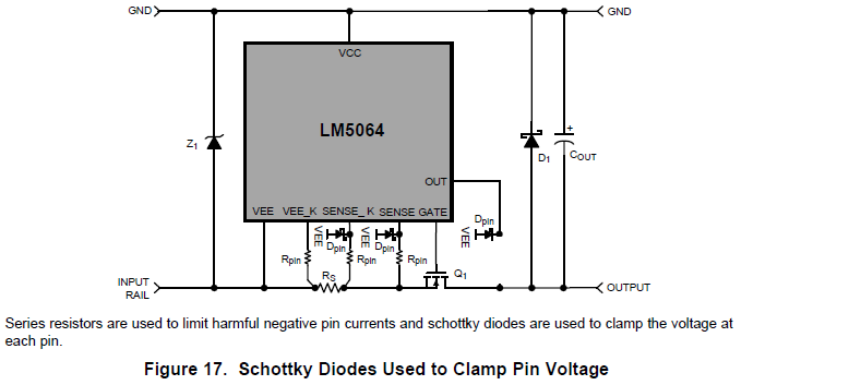
My customer considers to use LM5046 for -48V rail and designed like Figure17 as the following.
He adopt 30V schottky diode(Dpin) at OUT pin but it exceeds withstand voltage at power-up until Q1 FET become ON.
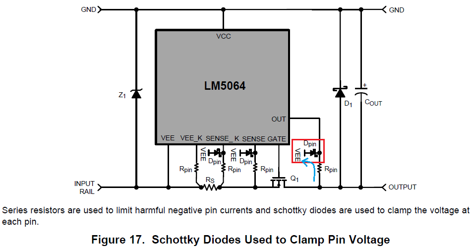


So he considers to increase the value of Rpin resistor to limit the voltage that applied cathode of Dpin.(to make voltage drop by design)
Is there maximum value for Rpin although the datasheet recommend 22Ω? 
I heard he can't change the schottky diode due to his design schedule...

Your advice would be appreciated.

Best Regards,
Yaita

  • Hi Team,

    I would like to ask additional question.
    My customer brings the other method into view about the issue.
    He considers to remove Rpin at the expense of Power Limiting as the following.
    Is it possible to remove it without introducing errors?


    I really appreciate if you advise me for two questions above.

    Best regards,
    Yaita / Japan disty

  • Hi Kensuke,

    We would not recommend the second figure shown where OUT is disconnected from the circuit.

    Power limiting is a critical feature of the device. Without it, it can be very difficult to create a design where the external MOSFET will not fail under stress conditions.

    We have design tools at www.ti.com/hotswap --> "Tools & Software" which can be used to check if the design would pass or fail without power limiting. We have a series of tutorial videos for each step of the design tool which can be viewed at www.ti.com/hotswap --> "Support & Training".

    Rpin for the sense lines are critical due to bias currents causing a voltage drop across Rpin resistor. For OUT, a larger Rpin resistor can probably be used, but that may not be a robust solution. For example, if there was a short circuit from GND to OUTPUT, then Dpin for OUT will still see a full Vin voltage across it.

    The description in the datasheet for Figure 17 mentions that the schottky diode for OUT must be rated to at least 100V. This would be the safest solution (to use a footprint compatible 100V schottky diode).

    Thanks!
    Alex